Electronic Contract Manufacturing Service Provider in California

What Is PCB Electronics and How Does It Work?

What Is PCB Electronics and How Does It Work?

PCB electronics forms the physical foundation of countless modern devices. A printed circuit board connects components through copper traces, pads, vias, and carefully planned layers. These parts work together like a compact road system for electrical signals. Power moves through designated paths. Data travels between chips, sensors, connectors, and control circuits.

Eric Bogatin, a respected signal-integrity expert, explains, “A signal is not just a voltage; it is a voltage between two conductors.” This principle matters in every PCB design. A trace carries more than current. Its width, length, spacing, and relationship with the ground plane can affect signal quality. Fast digital signals may reflect, weaken, or create unwanted noise when routing is careless.

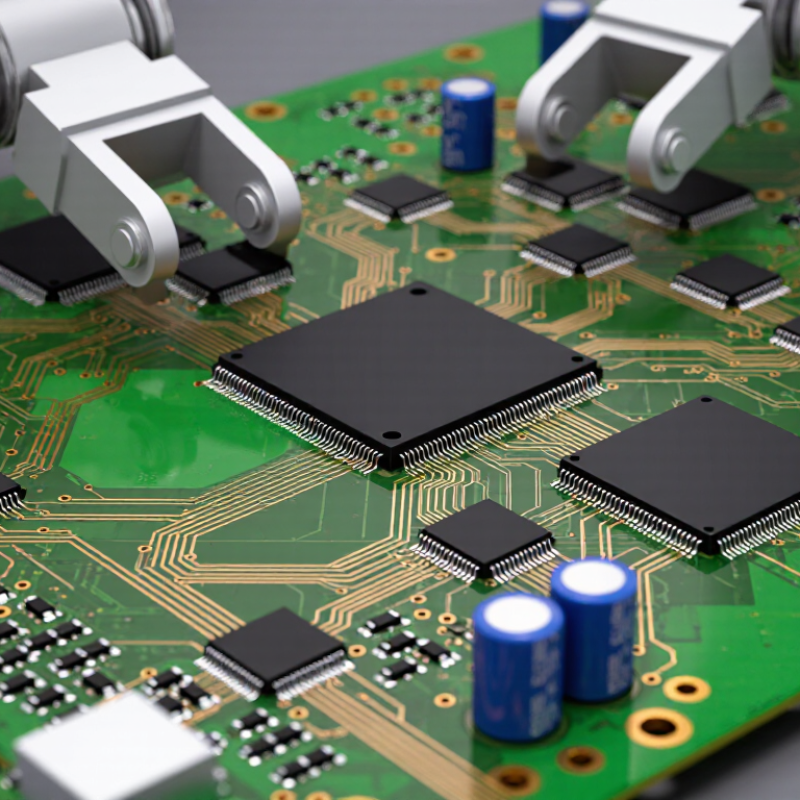
The process usually begins with a schematic. Engineers then convert that plan into a physical layout. The board may contain fiberglass, resin, copper foil, solder mask, and protective surface finishes. Components are placed and soldered onto the board, often using automated assembly equipment. Tiny details matter.

A small via can change performance.

Testing confirms whether the board behaves safely and reliably. Engineers inspect solder joints, measure electrical continuity, and evaluate heat under operating conditions. Still, a working prototype is not a perfect design. A board may pass an early test yet fail after repeated thermal cycling or vibration. That limitation deserves attention. Understanding PCB electronics means studying both its elegant structure and its practical weaknesses.
What Is PCB Electronics and How Does It Work?

Understanding the Meaning and Purpose of PCB Electronics

PCB electronics means electronic systems built around a printed circuit board. The board is not merely a flat holder for components. It routes power, carries signals, controls spacing, and supports mechanical connections. Copper traces act like mapped roads. Vias connect different layers, while solder masks protect exposed copper from accidental contact.

Its purpose becomes clear inside a small device. A sensor may send a weak signal through a copper trace to a processor. The processor then directs power toward a display, motor, or communication circuit. Resistors limit current, capacitors smooth voltage, and integrated circuits perform programmed operations. Everything must fit a defined electrical path. Small details matter.

Market data reflects this practical importance. Fortune Business Insights estimated the global PCB market at about USD 89.7 billion in 2023, with continued expansion expected through 2032. Prismark’s industry analysis also links growth to automotive electronics, computing, industrial controls, and connected equipment. These figures describe market value, not guaranteed product quality. That distinction matters.

In real engineering work, a PCB can fail because of heat, vibration, moisture, or an overlooked trace width. I have found that “working” is not enough; stable performance under stress is the harder target. A dense board may save space but complicate inspection and repair. A cheaper material may also increase long-term risk. Good PCB electronics balances conductivity, insulation, thermal behavior, manufacturability, and human error. That balance is imperfect.

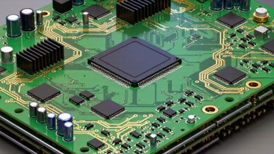
Key Components Found on a Printed Circuit Board

A printed circuit board is the physical framework that connects electronic parts. Its base is usually a rigid or flexible insulating material. Thin copper layers form traces, which carry electrical signals and power between components. Vias create vertical connections through the board. These small holes often look insignificant, but they can determine whether a compact design works reliably. The layout matters.

Resistors limit current and divide voltage. Capacitors store charge and reduce sudden voltage changes. Inductors manage changing current and help filter unwanted noise. Diodes allow current to move in controlled directions. Integrated circuits perform complex tasks, such as processing signals or controlling timing. Connectors provide links to batteries, sensors, displays, or other boards. A crystal or oscillator may provide a steady timing signal. Each part has a specific role, but its placement also affects performance.

During inspection, I look for clear trace spacing, firm solder joints, and correct component orientation. The solder mask protects copper from accidental contact. The silkscreen identifies part locations and polarity marks. Heat remains a practical concern. A power component may need extra copper area or thermal vias to spread heat. I have learned that a neat board is not automatically a good board. Sometimes, a tiny routing decision creates unexpected noise. That possibility deserves another measurement, not a guess. A missing ground connection can also hide beneath an otherwise impressive layout.

How Electrical Signals Move Through a PCB

What Is PCB Electronics and How Does It Work?

How Electrical Signals Move Through a PCB

A printed circuit board moves electrical signals through copper traces, vias, and component pads. A power source creates voltage, while electrons respond through the conductive path. The signal does not simply “flow” like water. Electric and magnetic fields carry information along the trace.

Picture a fast edge leaving a processor. It travels across a thin copper strip, crosses a plated via, and reaches a resistor. The trace width, dielectric thickness, and copper geometry control impedance. Poor routing can create reflections, ringing, and timing errors. Shorter is not always better.

The signal needs a return path.

At high frequencies, current follows the path of least impedance, often beneath the trace on a reference plane. A broken plane may force current around a gap, increasing electromagnetic noise. Industry design guidance commonly targets 50-ohm single-ended and 100-ohm differential routing, although each stack-up requires calculation.

The 2024 World Semiconductor Trade Statistics forecast projected global semiconductor sales of 611.2 billion dollars in 2024 and 687.4 billion dollars in 2025. More processing power means denser boards and faster transitions. IPC’s PCB technology guidance also emphasizes controlled impedance, clean power distribution, and verified materials for high-speed designs.

In practical testing, engineers use time-domain reflectometry to locate impedance changes. A connector, via, or sharp corner can become visible as a small discontinuity. Simulation helps, but it can miss manufacturing variation. That gap deserves attention. Copper roughness, resin thickness, and drilling tolerance can alter real signal behavior.

The Step-by-Step Process of PCB Operation

A PCB, or printed circuit board, is the physical platform that connects electronic components. Its operation begins when power reaches the board through an input connector. Copper traces then guide controlled current toward resistors, capacitors, processors, sensors, and other devices. The board’s layers separate power, signals, and ground. This structure reduces interference and supports stable performance.

The process is practical and sequential. First, a voltage regulator adjusts incoming power to safe levels. Next, capacitors smooth sudden electrical changes. A controller receives signals, processes instructions, and sends outputs through copper pathways. Finally, connectors transfer data or power to another circuit. IPC’s 2024 Electronics Industry Trends report identified supply-chain resilience and product reliability as continuing industry priorities. That matters because one weak solder joint can interrupt the entire signal path. The sequence looks clean on paper, but real boards can behave differently under heat, vibration, or electrical noise. Engineers must test those conditions rather than trust design software alone.

Tips: Keep traces short near high-speed components. Use wider copper paths for higher current. Check grounding carefully. A misplaced component can create heat, noise, or failure. The 2024 Global Electronics Association industry outlook also highlighted ongoing demand for advanced electronics manufacturing, while market analyses from Prismark continued to track strong growth in high-density interconnect and advanced packaging. These trends show why inspection, thermal testing, and controlled assembly are becoming more important. A useful design review should ask one uncomfortable question: what happens when the circuit is not operating perfectly?

What Is PCB Electronics and How Does It Work?

Typical Voltage Levels Through a PCB Operation Path

A PCB routes electrical power and signals through conductive copper traces, components, and connection points. This representative path shows common nominal voltage levels: a 12 V input is regulated to 5 V and 3.3 V rails, while a processor core may operate near 1.2 V. Actual values depend on the circuit design.

Common PCB Types and Their Everyday Applications

What Is PCB Electronics and How Does It Work?

A printed circuit board, or PCB, connects electronic components through copper pathways. These pathways carry power and signals across a compact, organized surface. In repair work, the board often reveals its purpose through connectors, chips, and mounting holes. A single-sided PCB has copper traces on one side. It suits simple devices such as basic timers, toys, and small control panels. Double-sided boards support denser circuits and appear in household appliances, measuring tools, and lighting equipment.

Multilayer PCBs contain several bonded copper layers. They handle complex products, including computers, medical instruments, communication equipment, and industrial controllers. Flexible PCBs bend inside cameras, wearable devices, and moving hinges. Rigid-flex boards combine firm sections with bendable connections. This design saves space, but it can increase manufacturing and inspection demands. The boundaries are not always neat. A compact board may use several types together.

Tips: Match the PCB type to heat, movement, moisture, and electrical load. Inspect solder joints under magnification. Look for darkened areas, lifted pads, or cracked traces. Keep cable pressure low near flexible sections. A small mistake matters. Designers also need controlled spacing between conductive paths. This reduces short-circuit risks and improves reliability. Still, laboratory testing cannot perfectly predict years of vibration or humidity. Real-world conditions deserve careful review.

What Is PCB Electronics and How Does It Work? - Common PCB Types and Their Everyday Applications

A printed circuit board (PCB) mechanically supports electronic components and electrically connects them through conductive copper traces, pads, vias, and other features.

PCB Type Typical Construction How It Works Main Advantages Common Everyday Applications Important Design Considerations
Single-Sided PCB One copper layer bonded to an insulating substrate, usually with components mounted on the opposite or same side. Electrical current travels between component pads through copper traces on one side of the board. Low cost Simple production Easy to assemble Basic power supplies, calculators, simple timers, lighting controls, low-complexity consumer electronics, and some household appliances. Routing space is limited, and wire jumpers or careful component placement may be needed for more complex circuits.
Double-Sided PCB Two copper layers separated by an insulating core, with plated through-holes or vias connecting the layers. Signals and power can move between the top and bottom copper layers through vias, allowing more compact routing. Higher routing density Moderate cost Better layout flexibility Power adapters, audio equipment, industrial controls, security devices, motor controllers, and general-purpose electronic instruments. Clearance, via placement, solderability, and thermal management must be controlled on both sides of the board.
Multilayer PCB Three or more copper layers separated by dielectric insulating layers and laminated into one board. Dedicated signal, power, and ground planes provide controlled interconnections between components and internal layers. High density Improved signal integrity Efficient grounding Computers, networking equipment, medical instruments, industrial automation systems, automotive control units, and advanced consumer electronics. Layer stack-up, impedance control, heat dissipation, via structures, electromagnetic compatibility, and manufacturing cost are critical.
Rigid PCB Built on a solid, non-flexible substrate that maintains a fixed shape during normal use. Components and conductive traces remain mechanically supported by the rigid laminate while signals travel through the copper pattern. Strong support Stable dimensions Broad availability Televisions, desktop computers, appliances, test equipment, control panels, chargers, and fixed electronic modules. Board outline, mounting holes, vibration resistance, connector placement, thermal expansion, and enclosure compatibility must be considered.
Flexible PCB Uses thin flexible dielectric films and flexible copper conductors that can bend or fold within specified limits. Electrical paths remain active while the board conforms to a curved or moving mechanical structure. Lightweight Space saving Supports movement Wearable devices, camera modules, compact displays, printer mechanisms, medical sensors, and connections between moving assemblies. Bend radius, repeated flexing, stiffeners, strain relief, conductor geometry, and protection against tearing are essential.
Rigid-Flex PCB Combines rigid board sections with flexible sections in one integrated laminated structure. Rigid areas hold components, while flexible sections route signals through bends between separate mechanical areas. Fewer connectors Compact assembly High reliability Portable instruments, aerospace electronics, compact medical equipment, robotics, cameras, and devices with hinged or folded structures. Transition zones, bend requirements, layer alignment, material compatibility, assembly tooling, and repairability require careful planning.
HDI PCB High-density interconnect construction using fine lines, small pads, microvias, and often sequentially built-up layers. Microvias and fine-pitch routing create short, dense connections between closely spaced components and internal layers. Very high density Shorter connections Smaller form factor Smartphones, compact computing devices, miniature cameras, advanced wearable electronics, and high-density control modules. Trace width, spacing, microvia reliability, material selection, fabrication tolerances, heat flow, and inspection capability are important.
Metal-Core PCB Contains a metal base, commonly aluminum or copper, beneath the dielectric and copper circuit layer. Heat generated by components transfers through the dielectric to the metal core and then into a heatsink or surrounding structure. Improved heat spreading Mechanical strength Thermal stability LED lighting, power converters, motor drives, automotive lighting, battery systems, and other heat-producing electronic assemblies. Thermal resistance, electrical isolation, mounting contact, coefficient of thermal expansion, and insulation thickness must be evaluated.
RF and Microwave PCB Uses controlled dielectric materials and carefully designed transmission lines for high-frequency signals. Signal paths are designed with controlled impedance so high-frequency energy travels with limited reflection and loss. Controlled impedance Low signal loss High-frequency performance Wireless communication equipment, radar systems, satellite electronics, navigation units, wireless sensors, and radio-frequency test instruments. Dielectric constant, loss tangent, trace geometry, grounding, shielding, connector transitions, surface finish, and layout symmetry are significant.
Aluminum-Backed LED PCB A thermally conductive metal-backed board designed to mount LED packages and transfer heat away from them. Electrical traces power the LEDs while the backing layer conducts heat toward a heatsink or mounting surface. Good thermal control Longer component life Compact lighting design LED bulbs, light strips, outdoor luminaires, vehicle lighting, signage, and high-power indoor lighting fixtures. LED junction temperature, thermal interface quality, current distribution, optical spacing, and insulation between copper and metal are key factors.
High-Voltage PCB Designed with increased spacing, suitable insulation systems, and materials rated for elevated voltage differences. Conductive paths carry power while creepage, clearance, slots, and insulation barriers limit arcing and unwanted leakage. Electrical safety Insulation control Reliable power handling Inverters, power supplies, battery chargers, industrial drives, energy conversion equipment, and high-voltage measurement systems. Working voltage, transient voltage, creepage, clearance, pollution level, insulation material, humidity, and safety testing must be addressed.
How a PCB works in general: Components are mounted on designated pads, and copper traces provide conductive paths between them. Vias connect different copper layers, power and ground structures distribute energy, and the completed circuit performs functions such as processing signals, controlling motors, managing power, or communicating data.