What Is a Printed Circuit Board and How Does It Work?
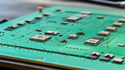
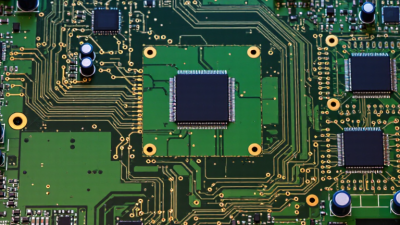
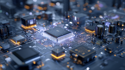
A printed circuit board is the quiet platform behind nearly every modern electronic device. It holds components in place and connects them through carefully designed copper pathways. These pathways carry electrical signals and power between chips, resistors, connectors, and sensors. Without this organized structure, a smartphone would become a loose collection of fragile wires.
The idea is not entirely new. Paul Eisler, the inventor of the printed circuit board, described it as “the biggest invention since the invention of the wheel.” His statement may sound dramatic, yet a circuit board can make complex technology smaller, faster, and more dependable. A typical board includes insulating layers, copper traces, drilled vias, solder mask, and printed markings. Each detail has a practical purpose. Copper conducts electricity. Vias connect different layers. Solder mask helps prevent accidental shorts.
The process begins with a circuit design, often created with electronic design automation software. Manufacturers then transfer that design onto laminate, etch unwanted copper, drill holes, and assemble components. Heat and pressure matter. So does cleanliness. A tiny manufacturing defect can interrupt an entire signal path.
This explanation has limits. Not every printed circuit board follows the same structure or manufacturing method. High-speed boards require different controls than simple consumer boards. That distinction is easy to overlook. Still, the basic principle remains clear: the board transforms an abstract circuit diagram into a physical, working system. Understanding that connection makes troubleshooting and design decisions more practical.
What Is a Printed Circuit Board?
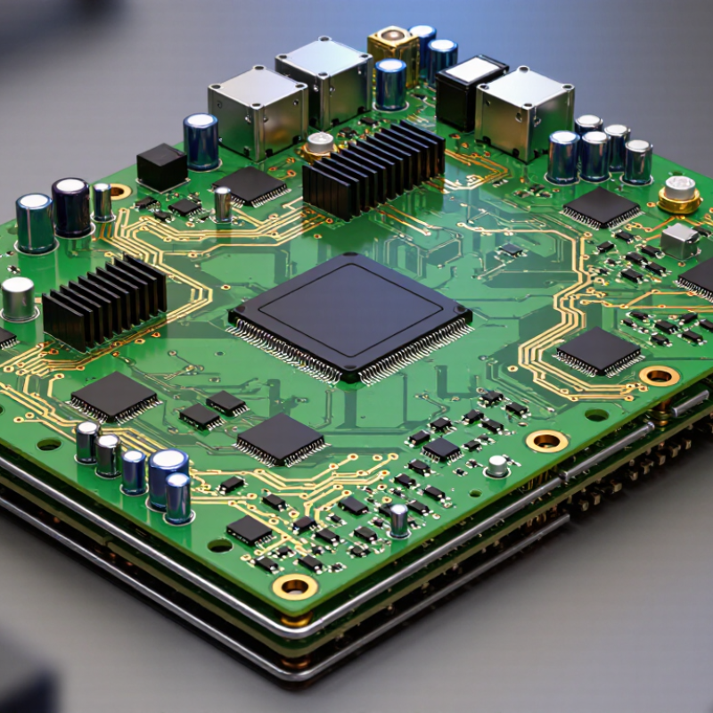
A printed circuit board, or PCB, is the physical platform that connects electronic components. It is usually a flat panel made from insulating material, with thin copper pathways attached to its surface or placed inside. These pathways, called traces, carry electrical signals and power between components. Small holes, known as vias, can link copper paths across different layers.
A PCB is more than a piece of green material. It may contain two layers or many carefully aligned layers. Components such as resistors, capacitors, connectors, and integrated circuits are mounted on its surface. Solder holds their leads or contacts in place. The board also includes pads, drilled holes, and protective coatings that help prevent accidental contact and corrosion. In practical inspection, damaged traces may appear as fine scratches, darkened areas, or lifted copper near a solder joint. Not quite. Appearance alone can mislead.
When power enters the board, traces guide current to specific circuit sections. Components then control, store, filter, or transform that electrical energy. Signals may travel between sensing, processing, and output areas in fractions of a second. The layout affects heat, noise, signal quality, and repairability, so spacing is not merely cosmetic. It is easy to oversimplify. A PCB does not think by itself; its components work together to perform intended functions. Designers must consider temperature, mechanical stress, manufacturing tolerances, and safe electrical separation. A visual check helps, but it cannot replace electrical measurements and controlled inspection.
What Are the Main Parts of a PCB?
What Is a Printed Circuit Board and How Does It Work?
A printed circuit board, or PCB, is a layered platform that connects electronic components. Its substrate provides mechanical strength and electrical insulation. Common materials include fiberglass and resin. Copper foil forms traces, pads, and planes. Traces act like tiny roads for current. Pads receive component leads or surface-mounted terminals. Vias connect copper paths between layers. They are small, plated holes.
The solder mask covers most copper and helps prevent accidental bridges. The silkscreen adds reference marks, polarity symbols, and inspection labels. Components, connectors, and integrated circuits sit on the board’s surface. Together, these parts control power distribution and signal movement.
According to Grand View Research, the global PCB market reached about 89.7 billion dollars in 2023. Precedence Research estimates continued expansion toward more than 150 billion dollars by 2032. The figures differ because researchers use different market boundaries. That difference deserves attention.
In practical inspection, failed boards often reveal simple weaknesses. A narrow trace may overheat under unexpected current. A poorly placed via can increase signal interference. An incomplete solder-mask opening can prevent reliable assembly. IPC design guidance repeatedly emphasizes spacing, impedance control, thermal management, and manufacturability. These details matter more as boards become denser. A PCB can look clean and still perform poorly. Designers sometimes focus too heavily on routing and overlook return-current paths. That mistake is easy to make.
How Are Printed Circuit Boards Manufactured?
Printed circuit boards begin as copper-clad laminate, usually reinforced with woven glass and epoxy resin. Engineers transfer the circuit design onto the copper surface using imaging film or laser direct imaging. Exposed copper is etched away, leaving narrow conductive tracks. A 2024 report from The Business Research Company valued the global PCB market at more than 80 billion US dollars, reflecting demand for denser and more reliable boards.
Manufacturing continues through drilling, plating, solder-mask coating, and surface finishing. Computer-controlled drills create holes for component leads and plated vias. Copper plating then connects several board layers through these tiny openings. Automated optical inspection checks line width, registration, and surface defects. IPC process standards guide many production controls, but inspection cannot replace careful engineering judgment. A small alignment error can break an entire signal path.
Electrical testing follows assembly preparation. Test probes verify continuity and isolation, while thermal stress testing exposes weak bonds. According to SEMI’s 2024 semiconductor industry materials report, advanced electronics require tighter manufacturing tolerances and more complex interconnections. That pressure reaches PCB fabrication directly. Still, published market forecasts differ because researchers define “PCB market” differently. This is worth remembering. A clean factory floor also does not guarantee a perfect board; humidity control, operator decisions, and material storage can quietly affect reliability.
What Is a Printed Circuit Board and How Does It Work?
A printed circuit board (PCB) mechanically supports electronic components and electrically connects them through copper traces, vias, and conductive layers. The chart shows a representative four-layer PCB stack-up used during multilayer board manufacturing.
How PCB manufacturing uses these layers: copper foil is laminated to insulating materials, circuit patterns are transferred and etched, drilled holes are plated to form vias, and a solder mask is applied to protect the finished copper circuitry.
How Does a PCB Work in an Electronic Device?
A printed circuit board works as the electrical foundation of an electronic device. It holds components in fixed positions and connects them with thin copper traces. Power enters through a connector, then travels across these paths to reach regulators, processors, sensors, and memory circuits. The board does not create the signal. It directs and controls its movement.
Small holes called vias connect copper layers inside a multilayer board. A ground plane gives current a stable return path and can reduce electrical noise. Solder joins each component to copper pads, while the solder mask protects nearby traces from accidental contact. During operation, a processor may send a low-voltage signal through several traces before another circuit interprets it as data, sound, or a motor command.
Practical inspection reveals more than a diagram.
A cracked solder joint, loose connector, or overheated trace can interrupt power without visible damage. Technicians often check voltage at several test points instead of guessing from symptoms. A clean board can still contain a design weakness. Poor spacing may cause interference, and a narrow power trace may heat under heavy current. Even reliable calculations need testing because real materials, temperature, and assembly quality vary.
What Are the Different Types and Applications of PCBs?
Printed circuit boards, or PCBs, are the structured pathways behind modern electronics. They connect components through copper traces, pads, and drilled vias. Their type depends on space, heat, movement, and signal speed. A single-layer PCB suits simple controls. Multilayer boards support dense computers and communication equipment. Flexible PCBs bend inside cameras, medical sensors, and wearable devices. Rigid-flex designs combine both advantages, but they cost more and require tighter manufacturing control.
Applications continue to expand. Automotive systems use PCBs for battery monitoring, lighting, safety sensors, and navigation. Industrial machines need robust boards that tolerate vibration and temperature changes. Consumer electronics favor thinner designs with higher component density. Fortune Business Insights’ 2024 PCB market report valued the global market at about 83.21 billion US dollars in 2023. It projects strong growth through 2032. That estimate is useful, but forecasts can shift with material prices, regional demand, and supply disruptions. A board that works in a laboratory may fail inside a hot vehicle.
Tips: Choose the PCB type after defining temperature, bending, voltage, and repair needs. Do not select by price alone. Review trace width, insulation spacing, and thermal paths early. IPC’s 2023 World PCB Production Report shows how significant Asian manufacturing remains in global PCB production, yet regional concentration can increase delivery risk. Engineers should request material certificates and electrical test records. Small documentation gaps often become expensive field problems.