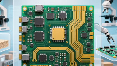
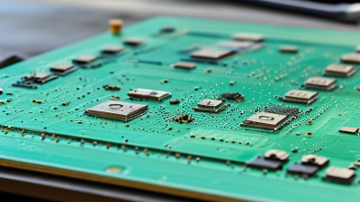
What Is a PCB Printed Circuit Board?
A pcb printed circuit board is the physical platform behind modern electronic products. It connects components through copper traces, plated holes, and carefully engineered insulating layers. Inside a smartphone, those traces may be thinner than a human hair. In an industrial controller, they may carry high current beside sensitive signals. The board is not merely a green plate. It is a designed electrical system.
Industry data shows why this subject matters. According to Fortune Business Insights’ Printed Circuit Board Market report, the global market was valued at approximately USD 83.25 billion in 2024. The report projects continued growth through 2032, supported by electric vehicles, telecommunications, automation, and consumer electronics. MarketsandMarkets also identifies high-density interconnect, flexible circuits, and multilayer boards as important growth areas. Different reports use different methods. That difference deserves attention.
Dr. Hayao Nakahara, a respected PCB industry analyst, has described the PCB as “the heart of electronics.” The phrase is simple. It remains useful. A board routes power, controls signals, supports components, and influences product reliability. Engineers must consider impedance, thermal movement, materials, assembly defects, and repair access. IPC standards provide widely used guidance for design, fabrication, and acceptance.
Still, no single standard guarantees a perfect board. Field experience matters. A design can pass inspection yet fail after vibration, moisture, or repeated heating. This is where careful testing becomes essential. Understanding the pcb printed circuit board begins with its structure, but it should end with evidence from real operating conditions.
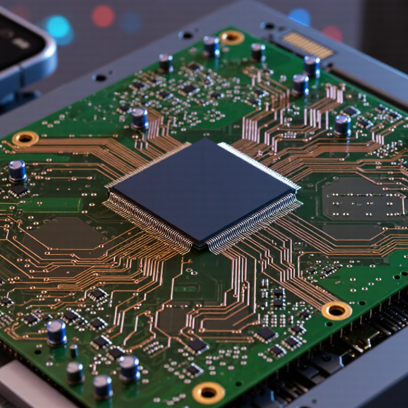
A printed circuit board, or PCB, is a structured platform for electronic components. It uses copper pathways, insulating layers, and drilled holes to connect parts electrically. Instead of loose wires, a PCB guides power and signals through planned routes. Its core purpose is practical: hold components securely, control connections, and support repeatable assembly. A small sensor board may contain only one copper layer. A computer control board can contain many layers, pressed tightly together.
In daily engineering work, the board also manages heat, spacing, and mechanical stress. Designers check trace width, current capacity, signal timing, and clearance before production. IPC design guidance commonly links these decisions to reliability and manufacturing class.
Industry data shows why this matters. The 2024 Global PCB Industry Report from Prismark estimated worldwide PCB sales at roughly 70 billion US dollars in 2023. Forecasts from leading market research groups place the sector on a steady growth path through 2030, supported by vehicles, communications equipment, and industrial electronics.
Numbers can mislead.
A larger market does not guarantee a better board. Poor grounding, weak solder joints, or excessive heat can still cause failure. My own practical view is that PCB quality begins with simple decisions: clean routing, suitable materials, and realistic testing. The board is not merely the green plate. It is the physical system that makes an electronic idea repeatable, inspectable, and usable.
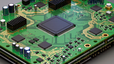
A printed circuit board, or PCB, connects electronic components through carefully designed copper pathways. In practical assembly work, its layout often determines whether a device works reliably. Common components include resistors, capacitors, diodes, integrated circuits, connectors, and switches. Each part has a specific electrical role. A resistor limits current, while a capacitor stores and releases energy. Tiny solder joints hold these parts to copper pads on the board. They look simple, but poor joints can cause intermittent failures.
A PCB usually contains several functional layers. The substrate provides mechanical support and electrical insulation. Many boards use a rigid insulating core between copper layers. Copper traces carry signals and power across the surface or inside the board. Solder mask covers most exposed copper and helps prevent accidental short circuits. Silkscreen markings identify components, polarity, test points, and connector positions. In a multilayer PCB, internal power and ground planes reduce noise and shorten current paths. Layer alignment must remain precise. A small registration error can weaken a connection.
During inspection, technicians check trace width, pad condition, solder quality, and drilled holes. They also compare the finished board with its design files. A board may pass an early test and still fail after heating or vibration. That is an important weakness in simple testing. I have found that visual checks alone can miss hidden defects. Electrical testing, controlled manufacturing, and clear documentation provide stronger evidence of reliability. Even a clean-looking PCB deserves careful review.
A printed circuit board, or PCB, forms electrical connections through patterned copper layers. The board begins with a rigid insulating core, often reinforced with woven glass. Copper foil covers its surface. During manufacturing, imaging and etching remove unwanted copper, leaving narrow traces, pads, and larger power areas.
These copper paths act like controlled roads for electricity. A trace connects a component pad to another destination. A plated through-hole, called a via, links copper layers through a drilled channel. Its inner wall receives a thin copper coating. Solder then bonds component leads or surface contacts to the pads. The connection must remain continuous, clean, and mechanically stable. Small defects can interrupt current or create heat.
Industry figures show why this process demands precision. Grand View Research valued the global PCB market at approximately 89 billion US dollars in 2023, with continued growth expected through the decade. IPC reliability guidance also emphasizes conductor spacing, hole quality, and copper thickness for dependable performance. These details are not decorative. They control resistance, signal loss, and insulation safety. In practice, the simple “copper road” analogy is incomplete. High-speed signals may need carefully calculated widths and spacing. Heat can also change resistance. A board that works on the first test may still age poorly. That is where my explanation becomes imperfect: real designs require measurement, material data, and repeated verification.
| PCB Element | Primary Function | How the Electrical Connection Is Formed | Typical Material or Structure | Representative Data | Key Design Considerations |
|---|---|---|---|---|---|
| Substrate | Provides mechanical support and electrical insulation between conductive layers. | Separates copper conductors while controlling spacing, impedance, and dielectric behavior. | Glass-reinforced epoxy laminate or another electrically insulating laminate. | Common multilayer dielectric thickness: approximately 0.10–0.40 mm per layer, depending on construction. | Dielectric thickness, thermal stability, moisture absorption, and dielectric constant affect signal performance. |
| Copper Layer | Carries electrical current and forms traces, planes, pads, and other conductive features. | Continuous copper areas are patterned by removing unwanted copper, leaving the required circuit paths. | Electrodeposited or rolled copper foil. | Common finished copper thicknesses include about 17–35 µm for standard external layers; heavier copper may be used for higher current. | Current capacity, heat dissipation, voltage drop, etching limits, and copper thickness must be considered. |
| Trace | Connects components, pads, vias, and copper planes across the board. | A copper trace provides a continuous low-resistance path between two or more circuit nodes. | Patterned copper on an outer or inner PCB layer. | Common trace widths range from approximately 0.10–0.30 mm in many general-purpose designs, but the allowable minimum depends on fabrication rules and current. | Width, thickness, length, spacing, current, temperature rise, and controlled impedance are important. |
| Pad | Provides a solderable connection point for component leads, terminals, or vias. | Solder joins the component termination to the copper pad, creating both mechanical attachment and electrical continuity. | Exposed copper, often protected by a surface finish. | Pad dimensions are normally specified from the component package footprint and manufacturing tolerance. | Pad size, solder mask clearance, thermal relief, component alignment, and solder-joint reliability are critical. |
| Through-Hole Via | Connects copper layers through the entire thickness of the board. | A plated copper barrel joins the via pad or annular ring on multiple layers. | Drilled hole with copper-plated walls and annular rings. | Typical finished hole diameters are approximately 0.20–0.80 mm, depending on board technology and application. | Drill size, aspect ratio, annular ring, plating thickness, and clearance from nearby conductors must be controlled. |
| Blind Via | Connects an outer layer to one or more internal layers without passing through the entire board. | A plated hole starts on an external layer and terminates at a specified internal layer. | Mechanically drilled or laser-formed plated structure. | Depth is limited by the selected layer pair and manufacturing process. | Useful for routing density, but requires tighter process control and usually increases fabrication complexity. |
| Buried Via | Connects internal layers without being visible on the external surfaces. | A plated hole is formed only between internal copper layers. | Plated internal-layer interconnection. | Located entirely within the board stack-up; it is not accessible from the outer surface. | Improves routing density but requires sequential fabrication and careful layer registration. |
| Annular Ring | Surrounds a drilled via hole and maintains a reliable copper connection. | The remaining copper around the hole provides the contact area between the plated barrel and the surrounding pad or plane. | Copper ring around the drilled opening. | Required width depends on drill tolerance, registration accuracy, and applicable design rules. | Insufficient annular ring can cause breakout and reduce connection reliability. |
| Copper Plane | Provides a low-impedance power or ground connection and helps distribute heat. | A large continuous copper region connects multiple points to the same electrical net. | Solid or hatched copper area on an internal or external layer. | Plane coverage is determined by board size, current requirements, thermal needs, and signal-routing constraints. | Plane continuity, return-current paths, clearances, thermal reliefs, and electromagnetic compatibility must be evaluated. |
| Solder Mask | Insulates and protects most copper surfaces while exposing areas intended for soldering. | Openings in the mask allow solder to contact pads, through-hole lands, and selected test points. | Polymer coating applied over the outer copper layers. | Typical cured thickness is approximately 10–30 µm, depending on application and process. | Mask clearance, registration, insulation spacing, and resistance to heat and chemicals affect assembly quality. |
| Surface Finish | Protects exposed copper and supports solderability. | Forms a protective metallic or chemical layer over exposed pads and other solderable copper areas. | Examples include tin-based, nickel-gold, or immersion-based finishes without relying on a particular supplier. | Finish selection depends on storage life, contact requirements, soldering method, and cost. | Flatness, oxidation resistance, thickness uniformity, solderability, and compatibility with assembly processes are important. |
| Solder Joint | Creates the final connection between a component termination and a PCB pad. | Molten solder wets the exposed pad and component surface, then solidifies into a conductive joint. | Lead-free or other qualified solder alloy applied by reflow, wave, selective, or hand soldering. | Joint quality is evaluated by wetting, shape, coverage, voiding, alignment, and mechanical integrity. | Pad geometry, thermal profile, solder volume, component finish, cleanliness, and inspection criteria influence reliability. |
| Layer Stack-Up | Defines the arrangement of signal, power, ground, copper, and dielectric layers. | Vertical interconnections through vias combine with horizontal traces and planes to form the complete circuit. | Single-sided, double-sided, or multilayer construction. | Common constructions include 1, 2, 4, 6, or more conductive layers, selected according to routing and performance needs. | Layer count, symmetry, impedance control, power integrity, thermal management, and manufacturability must be balanced. |
Note: The numerical values shown are representative engineering ranges rather than universal manufacturing limits. Actual values depend on the PCB stack-up, electrical requirements, component packages, and the selected fabrication process.
A printed circuit board (PCB) connects electronic components through copper paths on an insulating base. It controls signal routes, power delivery, and component placement inside a device. Common choices include rigid, flexible, rigid-flex, single-sided, double-sided, and multilayer boards.
Rigid PCBs suit control panels, appliances, instruments, and most stationary electronics. Their solid structure supports connectors, heat-producing parts, and repeated assembly.
Flexible PCBs bend around hinges, displays, cameras, or compact battery compartments. They reduce wiring and save space, but sharp folds can damage copper.
Rigid-flex boards combine stable mounting areas with bendable links. They often fit medical instruments, aerospace controls, and compact industrial equipment.
Single-sided boards keep routing simple and costs lower. Double-sided boards provide more connection space. Multilayer designs handle dense processors, memory, and high-speed signals.
PCB selection depends on current, voltage, heat, vibration, bend radius, and production volume. A designer should inspect creepage distances, hole sizes, copper thickness, and solder reliability.
Small details matter. For example, a hot regulator may need wider copper and nearby airflow.
In practice, the cheapest board is not always the safest choice. Compact layouts can become difficult to repair when test points are omitted.
That mistake is easy to repeat.
Early prototypes should leave room for measurement, rework, and unexpected electrical noise.
What Is a PCB Printed Circuit Board?
A printed circuit board, or PCB, connects electronic components through copper pathways. Its design begins with clear electrical and mechanical requirements. Engineers define voltage levels, signal speeds, board dimensions, and mounting points. A schematic then shows how each component should connect. It is the circuit’s logical map.
PCB layout turns that map into physical geometry. Designers arrange components, route copper traces, and create a suitable layer stack-up. High-speed signals need controlled paths and careful spacing. Power areas require enough copper to manage heat. Designers also check drill sizes, clearances, solder mask openings, and connector positions. A first layout is rarely perfect. Small oversights can create costly revisions.
Manufacturing starts with design-for-manufacturing checks. The fabricator forms copper layers, drills holes, applies insulation, and adds protective surface finishes. The assembled board receives components through automated placement and soldering. Inspection may include optical checks, electrical continuity tests, and functional testing under operating conditions. I have found that clean documentation prevents many avoidable errors. However, test results can still expose assumptions that looked reasonable during design. A slightly shifted component, an incomplete footprint, or an overlooked heat path may require another prototype. Reliable production depends on repeated verification, not confidence alone.
The chart shows representative working-time ranges for the main stages of PCB design and manufacturing. Actual duration depends on board complexity, layer count, component density, prototype quantity, and testing requirements.
Typical process durations are expressed in working days and are intended for general planning of a standard prototype PCB project.