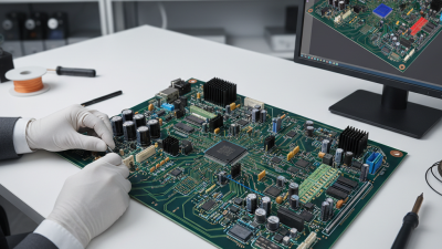
An electronic circuit board is the compact platform that connects, supports, and controls electronic components. Copper traces carry electrical signals across layered materials, while vias link different circuit paths. A smartphone board may fit beneath a fingernail. A server board can span several centimeters and contain thousands of connections.
The subject is larger than hardware alone. IPC’s electronics manufacturing reports track production activity, material demand, and supply-chain pressure across major regions. Prismark’s PCB Industry Forecast also shows how demand follows data centers, automotive electronics, industrial automation, and consumer devices. These reports suggest continued expansion, but growth is uneven. High-density boards require tighter tolerances, cleaner fabrication, and stricter inspection. A single hidden void can weaken a power connection. That detail matters.
PCB analyst Dr. Hayao Nakahara has said, “The PCB industry is a leading indicator of the electronics industry.” His observation remains useful because board orders often respond before finished-product sales become visible. Still, the phrase is not perfect. Inventory corrections, geopolitical disruption, and short product cycles can distort that signal. Understanding an electronic circuit board therefore requires more than naming its layers. It requires examining design intent, substrate choice, thermal behavior, manufacturing quality, and field reliability. This guide will explain those elements in practical terms, from the fiberglass core beneath the copper foil to the solder joints that must survive heat, vibration, and years of use.
What Is an Electronic Circuit Board?
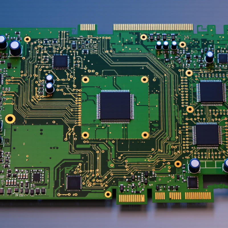
An electronic circuit board is a rigid or flexible platform that connects electronic components. Its basic function is more than holding parts in place. Copper traces carry electrical signals, while wider paths distribute power and ground. Vias connect different layers through small drilled holes. The substrate provides insulation and mechanical support. A solder mask protects exposed copper, and printed markings guide assembly and inspection. In practice, a bare board cannot perform a complete task. It needs components such as resistors, capacitors, sensors, or integrated circuits.
The board acts like a carefully organized road system. Signals travel along controlled routes, while power reaches each component through planned distribution paths. A well-designed layout can reduce noise, heat concentration, and signal loss. According to Fortune Business Insights, the global printed circuit board market was valued at approximately 83.82 billion dollars in 2023. The same report projects continued growth through 2032, reflecting demand across computing, vehicles, medical equipment, and industrial controls. These figures show the board’s industrial importance, but market size does not guarantee quality.
A practical inspection usually checks solder joints, trace spacing, connector alignment, and continuity. Thermal cycling can reveal weak joints that visual inspection misses. A board may look perfect and still fail under vibration or heat. That is an uncomfortable limitation. Design software also cannot replace engineering judgment. Clearances, material selection, grounding, and repair access require careful review. IPC workmanship standards and test procedures provide useful guidance, yet real operating conditions may expose assumptions that laboratory checks overlook.
An electronic circuit board is a structured platform that connects and controls electrical parts. Its copper traces act like narrow roads, carrying signals and power between components. The World Semiconductor Trade Statistics Autumn 2024 forecast reported global semiconductor sales of 627.6 billion dollars in 2024. That scale reflects the growing complexity behind modern boards.
Resistors limit current and protect sensitive circuits. Capacitors store electrical energy and reduce unwanted voltage changes. Diodes control current direction, while transistors switch signals or amplify them. Integrated circuits combine many functions inside one compact package. They may manage processing, timing, sensing, or communication. Small parts matter.
Connectors provide practical links to batteries, displays, cables, and other boards. Inductors help regulate power and filter electrical noise. A crystal oscillator can provide a stable timing reference. The board itself also matters: copper thickness, insulation, solder quality, and thermal design affect reliability. IPC technical guidance emphasizes that material selection and manufacturing control strongly influence long-term performance.
During inspection, I look for overheated solder joints, cracked components, and uneven coating near high-current areas. Heat leaves slowly. A clean surface can still hide a weak connection beneath a component. Designers sometimes prioritize compact layouts and underestimate repair access. That trade-off deserves more attention. The best component choice depends on voltage, current, temperature, vibration, and expected service life, not size alone.
(Sources: WSTS Autumn 2024 Forecast; IPC PCB technology guidance.)
What Is an Electronic Circuit Board?
How Electrical Signals Move Through the Board
An electronic circuit board guides electrical signals between components through carefully arranged copper paths. A source creates a voltage difference, while that difference pushes current through the circuit. The signal does not simply leap from one component to another. It follows traces, connection points, and return paths. In practice, electrons drift slowly, but the electrical effect can propagate much faster along the board.
A trace acts like a narrow conductor. Its width, thickness, and length influence resistance and heat. Vias carry signals between copper layers, while a ground plane provides a lower-impedance return route. When a signal changes rapidly, its return current may follow the path directly beneath the trace. This reduces unwanted radiation and crosstalk. Small design choices matter.
Measurement reveals the board’s real behavior. A probe placed carelessly can add capacitance and distort a fast waveform. I have found that a clean schematic does not guarantee clean signals. Reflections may appear when trace geometry and load impedance do not match. Noise can also enter through power connections, weak solder joints, or poor grounding. The board may work, but still need a closer look.
What Is an Electronic Circuit Board?
Common Types and Applications of Circuit Boards
An electronic circuit board supports components and connects them through conductive paths. It carries power, signals, or both. The most familiar types are single-sided, double-sided, and multilayer boards. Single-sided boards suit simple controls, lighting devices, and basic household equipment. Double-sided boards offer more routing space for compact products. Multilayer boards contain several copper layers, making them useful in computers, medical instruments, and industrial controllers.
Flexible circuit boards bend inside cameras, wearable devices, and moving equipment. Rigid-flex boards combine stable sections with bendable connections. Metal-core boards help remove heat from high-power lighting and control systems. In practical design work, board selection depends on current, frequency, space, heat, and expected service life. A visually neat layout can still fail if traces are too narrow or connectors receive repeated stress. That detail is easy to miss.
Tips: Check the board’s operating temperature and maximum current before installation. Keep moisture away from exposed conductors. Inspect solder joints under bright light. Uneven joints may signal weak connections. Leave room for testing and repair; compact layouts often look efficient but can become difficult to service. Choose protective coatings carefully, because some materials can interfere with connectors or future repairs. A circuit board is only one part of a reliable system. Its enclosure, wiring, cooling, and assembly quality matter too.
Printed circuit boards (PCBs) provide mechanical support and electrical connections for electronic components. The chart compares representative copper-layer configurations used in common PCB types.
Layer counts are representative configurations: single-sided and double-sided boards use one or two copper layers, while multilayer and HDI boards commonly use additional layers for denser routing and more complex applications.
What Is an Electronic Circuit Board?
Manufacturing, Testing, and Future Developments
An electronic circuit board connects components through carefully designed copper paths. Its manufacturing begins with laminate preparation, copper patterning, drilling, and surface finishing. Engineers control line width, spacing, and layer alignment during production. Small errors can create open circuits or unwanted electrical bridges. Dust matters. So does moisture.
Testing starts before final assembly. Automated optical inspection checks solder joints, component placement, and visible defects. X-ray inspection can reveal hidden voids beneath larger components. Electrical tests confirm continuity, insulation, and programmed functions. Thermal cycling exposes weak connections by repeatedly changing temperature. In practice, no inspection method catches everything. A clean visual result may still hide fatigue inside a plated hole. This is why manufacturers combine several tests and record traceable results.
Future boards will support denser circuits, faster signals, and smaller devices. Advanced materials may improve heat transfer and reduce signal loss. Embedded components could save space, but they may make repairs more difficult. Artificial intelligence can identify unusual defect patterns, although poor training data may create false alarms. Digital production records may connect design, assembly, and testing more accurately. Sustainable manufacturing also needs attention, including lower-energy processes, recyclable materials, and longer product life. Some promising ideas remain expensive or difficult to scale. Practical progress will depend on balancing performance, reliability, repairability, and environmental impact.
| Category | Data Dimension | Typical or Established Data | Why It Matters |
|---|---|---|---|
| Definition | Primary function | A printed circuit board mechanically supports electronic components and electrically connects them through conductive copper traces, pads, and other features. | The board provides both the physical structure and the signal or power pathways required by an electronic assembly. |
| Board Construction | Common layer configurations | Single-sided, double-sided, and multilayer constructions are widely used. Multilayer boards contain alternating conductive layers and insulating dielectric layers. | Additional layers allow more routing capacity and better power distribution within a smaller area. |
| Materials | Standard insulating substrate | Glass-reinforced epoxy laminate, commonly classified as FR-4, is widely used for general-purpose rigid boards. | The substrate provides electrical insulation, mechanical strength, and thermal stability during assembly and operation. |
| Conductors | Trace and plane material | Copper is the predominant conductive material. Copper thickness is commonly specified in ounces per square foot, with 1 oz copper measuring approximately 35 micrometres. | Copper thickness affects current-carrying capability, heat generation, impedance, and manufacturability. |
| Design | Typical design data | A board design normally includes a schematic, component footprints, copper routing, layer stack-up, drill data, solder-mask openings, and manufacturing documentation. | Complete design data enables fabrication, assembly, inspection, testing, and future maintenance. |
| Manufacturing | Basic production sequence | Typical steps include material preparation, imaging, copper pattern formation, etching or plating, drilling, solder-mask application, surface finishing, marking, routing, and final inspection. | Each process controls a different aspect of electrical performance, dimensional accuracy, or solderability. |
| Hole Formation | Drilled and plated holes | Through-holes pass through the entire board, while vias connect selected conductive layers. Plated holes receive a copper coating on their walls. | Hole geometry and plating quality determine reliable electrical connections between layers. |
| Surface Finish | Purpose of surface treatment | Common finishes include hot-air solder leveling, electroless nickel and immersion gold, immersion silver, and immersion tin. | The finish protects exposed copper and supports reliable soldering during component assembly. |
| Assembly | Component attachment methods | Surface-mount technology places components on board surfaces, while through-hole technology uses leads inserted into drilled holes. Reflow and wave soldering are common thermal processes. | The selected method affects component density, production speed, thermal exposure, and repair requirements. |
| Inspection | Automated optical inspection | Automated optical inspection checks visible features such as component presence, polarity, solder joints, trace patterns, and dimensional defects. | Optical inspection provides rapid, repeatable screening but cannot verify every hidden or internal connection. |
| Testing | Electrical test methods | In-circuit testing checks selected nodes and components using physical test access. Flying-probe testing uses movable probes and is suitable for lower-volume or frequently changing designs. | Electrical tests identify opens, shorts, incorrect connections, and selected component or assembly faults. |
| Testing | Functional testing | Functional testing operates the completed assembly under defined power, input, output, communication, and environmental conditions. | It confirms whether the product performs its intended system-level function rather than only checking physical connections. |
| Reliability | Common qualification stresses | Thermal cycling, humidity exposure, vibration, mechanical shock, solder-joint evaluation, and insulation-resistance testing are commonly used reliability checks. | These tests reveal failures caused by temperature changes, moisture, mechanical loads, and material aging. |
| Thermal Management | Heat-dissipation techniques | Common approaches include copper planes, thermal vias, heat sinks, metal-core constructions, and thermally conductive interface materials. | Effective thermal design helps limit component temperature and improves long-term reliability. |
| High-Speed Design | Signal-integrity considerations | High-speed boards require controlled impedance, appropriate layer stack-up, short return paths, differential-pair routing, and careful power-distribution design. | These practices reduce reflections, crosstalk, electromagnetic interference, and signal timing errors. |
| Miniaturization | Advanced interconnection structures | High-density interconnect boards can use microvias, fine traces, fine-pitch components, and sequentially built layers to increase routing density. | Higher interconnection density supports smaller and more capable electronic products but increases process-control demands. |
| Flexible Electronics | Flexible and rigid-flex boards | Flexible boards use bendable materials such as polyimide films. Rigid-flex constructions combine rigid sections with flexible interconnections. | These structures support compact packaging, repeated bending, and three-dimensional product layouts. |
| Sustainability | Environmental priorities | Important priorities include reducing material waste, recovering metals, improving energy efficiency, extending product life, and designing for repair or recycling. | Material selection and end-of-life planning can reduce the environmental impact of electronic products. |
| Future Development | Advanced materials | Research and development areas include low-loss dielectrics, improved thermal materials, embedded components, additive manufacturing, and substrates designed for higher-frequency operation. | These technologies aim to support faster data transmission, higher power density, and more compact electronic systems. |
| Future Development | Smart manufacturing | Connected production equipment, automated inspection, process data collection, digital twins, and machine-learning-based defect analysis are increasingly used to improve process control. | Data-driven manufacturing can improve yield, traceability, predictive maintenance, and production consistency. |