Electronic Contract Manufacturing Service Provider in California

What Is an Electronic Board and What Types Are There?

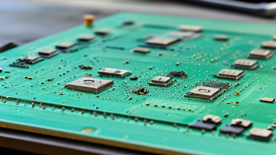
An electronic board is a platform that connects and supports components in an electrical or electronic device. It may carry tiny resistors and chips, larger connectors, or both. Copper traces form pathways between components, while the board’s shape and materials help it fit inside a product. In everyday use, people may call several different assemblies an electronic board, so the term can be broad. That distinction matters. A bare printed circuit board has conductive pathways but no installed components; a populated board has components attached and may perform a specific function.

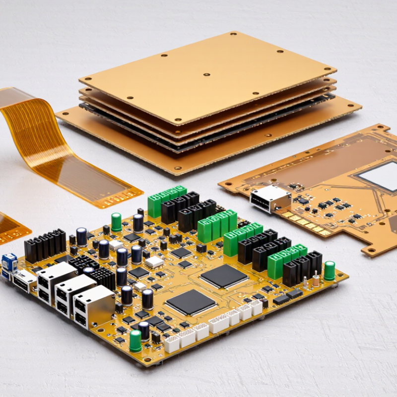
Board types vary by construction and purpose. Rigid boards are common in computers and household devices, while flexible boards bend to fit tight spaces, such as inside cameras or wearables. Rigid-flex designs combine both. Boards may also have one, two, or many conductive layers, depending on the number of connections and available space. Development boards, such as Arduino-compatible models, provide a convenient way to test circuits and software. Control boards manage functions in equipment, while display boards operate screens or indicators.

Look closely.

A connector’s position, a printed label, or a mounting hole can reveal practical design choices. Still, appearance alone rarely identifies a board’s full purpose; markings and product documentation offer better evidence. The sections ahead explain what electronic boards do, how major types differ, and which features matter when comparing them. The right choice depends on the device, environment, and task—not simply the board’s name.
What Is an Electronic Board and What Types Are There?

What Defines an Electronic Board? Substrates, Copper Paths, and Components

An electronic board is a platform that supports components and connects them electrically. Its substrate provides structure and insulation; common rigid boards use glass-fiber-reinforced epoxy. Flexible boards use bendable polymer films. The choice affects heat tolerance, stiffness, weight, and cost. No single substrate suits every design.

Copper foil is patterned into conductive paths, or traces, that carry signals and power between components. Components such as resistors, chips, and connectors are soldered onto copper pads. The board may also contain several copper layers separated by insulating material. That sounds tidy. Real layouts are messier: heat, tight spacing, and signal noise can force trade-offs. Prismark’s 2024 industry review estimated global PCB output at about US$68.3 billion in 2023, down roughly 15% from 2022. The scale is substantial, but that figure measures industry output, not board quality.

Tips: Inspect a board under good light. Look for the substrate, copper traces, solder pads, and mounted parts. On multilayer boards, some connections are hidden inside. Don’t assume every visible line is a surface trace.


How Board Layers Carry Signals: 1 oz Copper ≈ 35 μm Thick

A printed circuit board uses copper layers to route signals between components. On a typical board, thin copper traces form visible paths, while solid copper areas can serve as power or ground planes. The familiar “1 oz copper” label means roughly one ounce of copper per square foot. That mass corresponds to about 35 μm of copper thickness. IPC-4562, an industry specification for copper foil, describes foil by material and weight. The conversion is a useful shop-floor shorthand, not a promise about every finished layer.

A useful shorthand. Finished copper can differ from the starting foil because manufacturing may add copper during plating. Etching also shapes traces, leaving different widths and spacing across the board. These details matter: thicker copper can carry more current, but thickness alone does not determine safe current or signal quality. IPC-2152 provides empirical guidance for estimating trace current capacity and temperature rise. Its curves account for factors such as trace geometry and thermal conditions. A narrow trace beneath a warm component may behave differently from a broad trace with open airflow. That is easy to underestimate. Designers should check the finished stack-up and operating conditions, rather than treating “1 oz” as a complete electrical specification.

What Is an Electronic Board and What Types Are There? - How Board Layers Carry Signals: 1 oz Copper ≈ 35 μm Thick

Board or Layer Type Typical Construction How Signals Are Carried Copper Thickness Reference Common Uses and Notes
Single-sided rigid PCB One copper layer on a rigid insulating substrate Traces on the copper side connect components; the substrate electrically separates the traces from the opposite side. Common starting copper includes 0.5 oz (about 17.5 μm) or 1 oz (about 35 μm). Used for relatively simple, low-cost circuits. Routing is limited to one copper plane.
Double-sided rigid PCB Copper layers on both sides of a rigid core, joined by plated through-holes or vias Signals route on either side and can pass between layers through conductive vias. 1 oz (about 35 μm) is a common nominal starting-weight reference per copper layer. Offers more routing area than a single-sided board; often used in general-purpose electronics.
Multilayer rigid PCB Three or more copper layers separated by insulating dielectric material and bonded into one board Outer and inner signal layers carry routed traces; dedicated planes may distribute power or provide a ground reference. Vias connect selected layers. Copper weight is specified per layer. 1 oz ≈ 35 μm nominal copper thickness before considering processing and finished-board variation. Layer count and stack-up depend on routing density, electrical requirements, and mechanical constraints.
Flexible PCB One or more copper layers on a bendable dielectric film, commonly polyimide Copper traces carry signals through the flexible area; layer count and bend design affect routing and reliability. Copper thickness varies by design; thinner copper is often selected where repeated flexing is required. Used where space, weight, or movement makes a rigid board unsuitable. Bend radius and flex-cycle requirements matter.
Rigid-flex PCB Rigid board sections integrated with flexible circuit sections Signals travel across rigid and flexible regions using continuous or connected copper paths within the designed stack-up. Copper construction varies between rigid and flex regions; the flex area is designed to tolerate its intended bending. Can reduce connectors and cabling in compact assemblies, but requires careful mechanical and stack-up design.
Copper weight: 0.5 oz Nominal copper weight per square foot Forms the conductive traces and planes on a board layer. Approximately 17.5 μm nominal thickness A lighter copper option; actual finished trace thickness can vary with fabrication processes.
Copper weight: 1 oz Nominal copper weight per square foot Provides conductive material for signal traces, power paths, and copper planes. Approximately 35 μm nominal thickness A widely used reference value. Finished copper thickness may differ because of plating, etching, and manufacturing tolerances.
Copper weight: 2 oz Nominal copper weight per square foot Thicker copper can support higher-current paths and may affect trace geometry and spacing. Approximately 70 μm nominal thickness The required copper weight depends on current, temperature rise, board construction, and design rules.

Note: Copper-weight-to-thickness values are nominal conversions; finished copper thickness can vary by layer and manufacturing process.

Standard PCB Classes: Single-, Double-, and Multilayer Boards

A single-sided PCB has one copper layer, usually carrying straightforward connections beneath its components. Double-sided boards use copper on both faces, with plated holes linking the layers. Multilayer boards bond three or more conductive layers together, separated by insulating material. More layers can fit denser routing into a smaller footprint, but add manufacturing steps, cost, and thermal design challenges. Compact does not mean simple.

Prismark’s 2024 industry report placed global PCB production value at about $68 billion for 2023. That figure reflects many board types, not multilayer boards alone. Still, it shows the scale of the field. In practice, board choice depends on routing density, space, signal needs, and production volume—not layer count alone. I find layer count an imperfect shortcut: a carefully routed double-sided board can suit a design better than a crowded multilayer one.

Tips: Check the layer stack-up, copper thickness, and insulation specifications before comparing quotes. Ask how heat will escape near power components. One extra layer can help. Sometimes, it only adds cost.

Specialized PCB Types: Rigid, Flexible, and Rigid-Flex (IPC-6013)

Rigid printed circuit boards use stiff laminate to hold components in place and preserve geometry. They suit equipment with fixed layouts and steady mechanical support. Flexible boards use thin polymer film, often polyimide, to fold through a narrow enclosure or move with a joint. They save connectors and space. But repeated bending can still damage copper if the bend radius is too tight.

Rigid-flex boards join rigid component areas to flexible connecting sections. They can reduce cable assemblies, yet their layer transitions need careful design. IPC-6013 sets qualification and performance requirements for flexible and rigid-flex printed boards. It helps teams specify construction and acceptance criteria; it does not replace design reviews or testing. A practical check is to inspect the bend path, copper features, and stiffener edges together. Small details matter.

Market data gives context, not a design rule. Grand View Research’s Flexible Printed Circuit Board Market report estimated the global market at about US$20.4 billion in 2023 and projected 10.3% annual growth from 2024 to 2030. Flexible demand is rising. Still, choosing flex solely to make a board thinner can backfire. A simple rigid board may be more reliable when nothing needs to move. Conversely, a rigid-flex design can reduce assembly complexity, though it may be harder to repair. The right choice depends on motion, space, service access, and expected bending cycles.

How Boards Are Specified: Layer Count, Copper Weight, and IPC-4101 Materials

An electronic board is more than a flat support for components. Its layer count, copper thickness, and laminate material affect routing space, heat flow, and electrical performance. A two-layer board may suit a simple control circuit, while dense routing or controlled-impedance signals can require additional layers. More layers add capability, but also increase thickness and design complexity.

Copper weight is commonly stated in ounces per square foot. One ounce corresponds to roughly 35 micrometres of copper before processing. That is a useful reference, not a guarantee of finished trace thickness: etching and plating change the final geometry. Specify whether the value describes starting foil or finished copper, especially when narrow traces carry current or impedance must be controlled. Small wording gaps matter.

IPC-4101 identifies requirements for rigid-board base materials through material designations and related specifications. Engineers use the selected material’s construction and properties, such as glass-and-resin composition and thermal behavior, to match the board’s operating conditions. A higher glass-transition temperature may be appropriate for hotter assembly or service environments, but it does not solve every reliability concern. Check the complete stack-up, supplier data, and fabrication tolerances together. A specification can look complete and still leave room for interpretation.