Printed PCB Tips for Beginners How to Start Effectively?
In the world of electronics, mastering printed PCB design is essential for success. Renowned expert Dr. Alex Thompson emphasizes, “Every great innovation starts with a well-designed printed PCB.” For beginners, entering this field can feel daunting. The complexity of designs and the myriad of choices can sometimes lead to confusion.
Beginners often overlook the importance of planning. Creating a printed PCB without a clear roadmap might result in errors. It's easy to make mistakes in layout and component selection. Each misstep can lead to wasted time and resources. Acknowledging these potential pitfalls is crucial for growth and learning.
Hands-on practice plays a vital role in understanding printed PCBs. Experimenting with simple designs can lead to better knowledge. Beginners should not shy away from seeking advice and revisiting their designs. Embracing imperfections can pave the way to mastery in this intricate field.
Understanding Printed Circuit Boards (PCBs) and Their Importance
Printed Circuit Boards (PCBs) are essential components in modern electronics. They facilitate electrical connections and offer mechanical support for various electronic devices. According to a recent industry report, the global PCB market is expected to reach over $80 billion by 2026, growing at a CAGR of 4.5%. This highlights the significant role PCBs play in technology today.
Understanding PCBs involves recognizing their types and functions. Single-layer, double-layer, and multilayer boards each serve different applications. For beginners, it might be overwhelming to grasp these variations quickly. However, each type has its advantages and drawbacks. Beginners often underestimate the importance of quality design. Poorly designed PCBs can lead to defects and failures.
The fabrication process of PCBs can be intricate. Many newcomers face challenges with soldering techniques and component placement. Mistakes in these areas can result in malfunctioning devices. Research indicates that around 30% of prototype boards fail due to design issues. Learning from these experiences is key to improving. Embracing the complexity of PCBs can eventually lead to better designs and more reliable electronics.
Essential Tools and Materials for PCB Printing Beginners
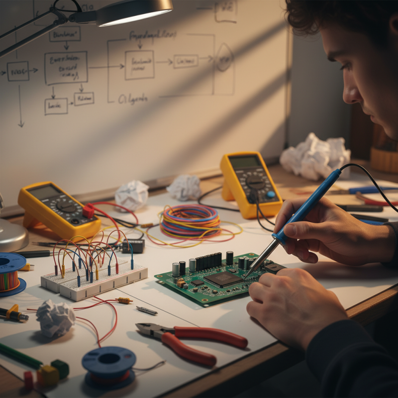
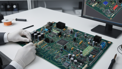
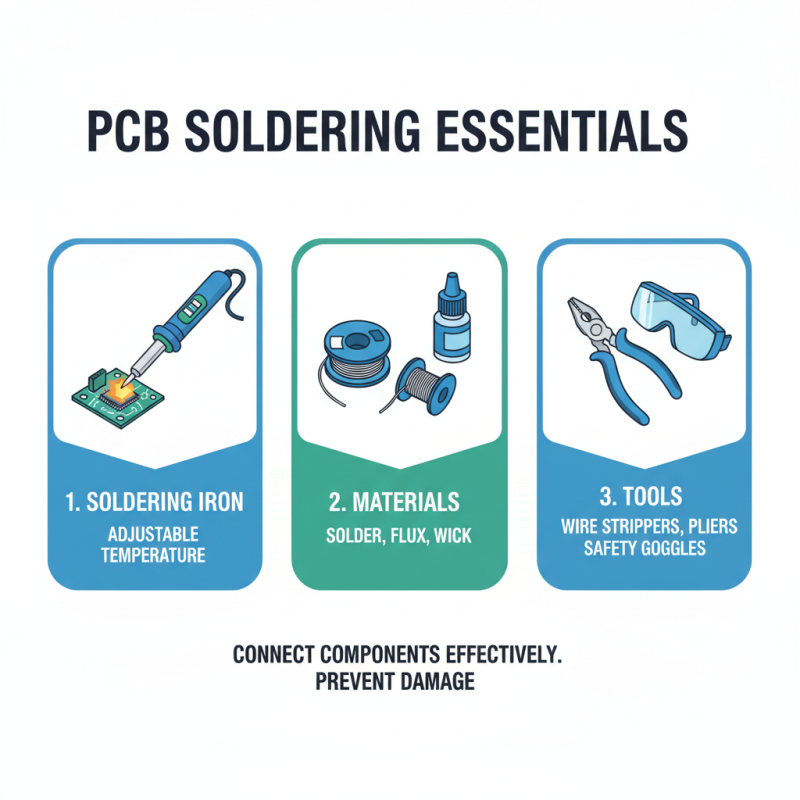
Getting started with printed circuit boards (PCBs) can be overwhelming. Knowing the essential tools and materials is crucial. A reliable soldering iron is a must-have. It allows you to connect components effectively. Make sure to choose one with adjustable temperature settings. That will help prevent damage to sensitive parts.
Another vital item is the PCB design software. There are many user-friendly options available. These simplify the design process for beginners. Don't forget to acquire a good quality copper-clad board. This will serve as your base for building prototypes. Additionally, purchase some etching solution and safety gear. Safety goggles and gloves are essential when handling chemicals.
You might face challenges while working on your first PCB. Mistakes happen, and that's part of the learning process. Sometimes, the etching may not go as planned. In these moments, reflect on your technique and adjust. Getting familiar with layering and component placement takes time. Embrace the trial and error approach, and you will improve. Each attempt will enhance your skills and confidence.
Step-by-Step Guide to Designing a PCB Layout
Designing a PCB layout can seem daunting for beginners. Start by familiarizing yourself with the components you'll use. Understanding the purpose of each part is crucial. According to industry reports, nearly 60% of design errors arise from incorrect component placement. Recognizing common mistakes can help.
Next, use software tools designed for PCB layout. These tools offer user-friendly interfaces, helping beginners visualize their designs. However, even these tools have limitations. For example, automatic routing may not always create the most efficient paths. Manual adjustments are often necessary to optimize performance.
Pay attention to the rules of design. Maintaining proper spacing between traces is vital to avoid interference. Data shows that a 10% increase in spacing reduces signal noise significantly. While it’s tempting to rush through the design, taking the time to double-check layout choices is wise. These small details can make a big difference in functionality. Beginners should embrace mistakes as part of the learning process.
PCB Design Process - Key Steps
Techniques for Effective PCB Printing and Assembly
When starting with PCB printing, understanding the right techniques is crucial. Choose a suitable printing method that aligns with your project. For beginners, screen printing might be easier to handle. It allows for precise control over ink application. However, the setup can be challenging. It often requires trial and error to achieve desired results.
Consider the materials used in your PCB assembly. Using high-quality substrates can make a significant difference. Pay attention to solder types as well. Not all solder works well with every board design. Be prepared for difficulties during the assembly phase. Sometimes components may not align perfectly. This can lead to frustrating errors.
Testing is essential after assembly. Conducting functional tests can highlight issues early. Don't be discouraged by initial mistakes; they are part of the learning curve. Document each step to avoid repeating errors. Continuous improvement is a key aspect of mastering PCB printing and assembly. With practice, your techniques will refine and enhance your projects.
Printed PCB Tips for Beginners How to Start Effectively?
| Aspect |
Tip |
Details |
| Design Software |
Choose User-Friendly PCB Software |
Utilize software like KiCad or Eagle for intuitive design processes. |
| Layout |
Keep Traces Short |
Minimize signal loss and interference by designing compact layouts. |
| Component Selection |
Choose Reliable Components |
Opt for components with a good reputation for reliability and durability. |
| Soldering |
Practice Good Soldering Techniques |
Learn proper soldering methods to avoid cold solder joints and shorts. |
| Testing |
Conduct Thorough Testing |
Run functional tests on PCB after assembly to ensure all connections are correct. |
| Documentation |
Keep Detailed Records |
Document your design process and any issues faced for future reference. |
Common Mistakes to Avoid When Starting with Printed PCBs
When starting with printed PCBs, many beginners make common mistakes that can hinder their progress. One frequent error is overlooking the importance of a well-structured design. Without a clear plan, you may end up with a circuit that is difficult to troubleshoot. Skipping the schematic phase leads to confusion later on, and mistakes can be costly.
Another pitfall is not considering the manufacturing limitations. Components can be too close together, leading to issues during fabrication. Beginners often underestimate the significance of proper spacing. In this case, less is more. Keeping designs simple can help avoid complications. It's vital to check the design rules of your fabrication house to ensure compatibility.
Additionally, neglecting to prototype before finalizing designs can prove disastrous. Rushing into production without testing can lead to significant failures. Build a prototype to discover flaws in your design. Expect imperfections and learn from them. Every misstep provides an opportunity for growth. Embrace these challenges as stepping stones in your PCB journey.