What is PCB Fab and How Does it Work in Electronics Manufacturing?
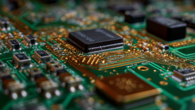
PCB fab plays a crucial role in electronics manufacturing. It encompasses various processes that transform raw materials into functioning printed circuit boards. These boards are essential for nearly all electronic devices today.
In a typical PCB fab, design files guide the entire process. These files dictate layout, component placements, and necessary specifications. All of this provides a roadmap for creating the hardware. However, the process can be complex and prone to errors. Mistakes in design can lead to costly revisions and delays. It’s essential to pay attention to detail during each step.
Understanding how PCB fab works can enhance the quality of electronic products. Each layer of the PCB has distinct purposes. Manufacturers must consistently assess their techniques to improve efficiency. Despite advancements, challenges remain. The industry often faces issues with material sourcing and production waste. Continuous improvement is vital for success in the PCB fab landscape.
Understanding PCB Fab: Definition and Importance in Electronics
PCB fabrication, often referred to as PCB Fab, is crucial in electronics manufacturing. It involves a complex process of creating printed circuit boards. These boards are the backbone of electronic devices, connecting various components. Understanding PCB Fab is essential for anyone involved in electronics.
The process begins with design. Engineers use specialized software to create layouts. These layouts guide the fabrication process. Then, materials like copper and fiberglass are used. Layers are etched and assembled. This results in a physical board that hosts all the necessary connections. Despite advancements, challenges remain. Not all designs translate seamlessly into effective PCBs.
Quality assurance is vital. Engineers and manufacturers must continuously test and refine their processes. Even minor errors in the fabrication process can lead to significant issues. Thus, meticulous attention to detail is necessary. Each PCB must be reliable and durable. This is essential for the functionality of the final product.
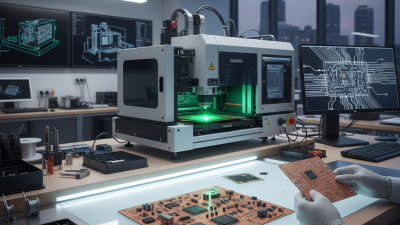
PCB Fabrication Process Overview
This chart illustrates the approximate time taken in hours for each step of the PCB fabrication process, highlighting the stages from design to final inspection, essential in understanding the importance of PCB fab in electronics manufacturing.
Key Processes in PCB Fabrication: From Design to Production
PCB fabrication is a complex process that transforms a design into a tangible circuit board. It starts with a detailed blueprint, created using specialized software. Designers create layers that will form the basis of the board. Each layer serves a specific function, like conducting electricity or insulating parts from each other. Once the design is ready, engineers prepare for production.
The first step involves printing the circuit patterns onto a substrate. This typically uses a photolithography process. Light exposure allows certain areas to remain exposed while others are protected. After that, a chemical etching process removes the unwanted material. This step can be tricky. Sometimes, mistakes happen, leading to faulty connections. Next comes the addition of holes for components. Drilling must be precise, as errors can result in malfunctioning boards.
Once the board is patterned and drilled, it undergoes plating. This adds a thin layer of copper to the exposed areas. During this phase, quality checks are essential. Any oversight can impact the entire production. After plating, the surface is cleaned and prepared for solder mask application. The final touches involve adding silkscreen for labeling and protection. Each stage has its challenges. Proper planning and execution can minimize problems, yet mistakes still occur. The journey from design to production is intricate, requiring attention to detail at every step.
Materials Used in PCB Manufacturing: Types and Their Impact
In PCB manufacturing, the choice of materials is crucial. Different substances affect performance, durability, and cost. Common substrates include FR-4, a glass-reinforced epoxy that balances cost and performance. It is widely used. However, it might not handle high frequencies well.
Another option is polyimide, known for its flexibility and heat resistance. This makes it suitable for flexible PCBs, but it tends to be more expensive. Then there's Rogers material, designed for high-frequency applications. Its unique properties enhance signal integrity but can significantly increase production costs.
Using the right material can impact the final product's reliability. This often requires testing prototypes. Manufacturers should be cautious and reflective about material choices. Overlooking material properties can lead to failure in applications or excessive costs. Balancing performance and budget is essential but challenging. Each decision mattered and has been worth reflecting on for many.
Industry Standards and Quality Control in PCB Fabrication
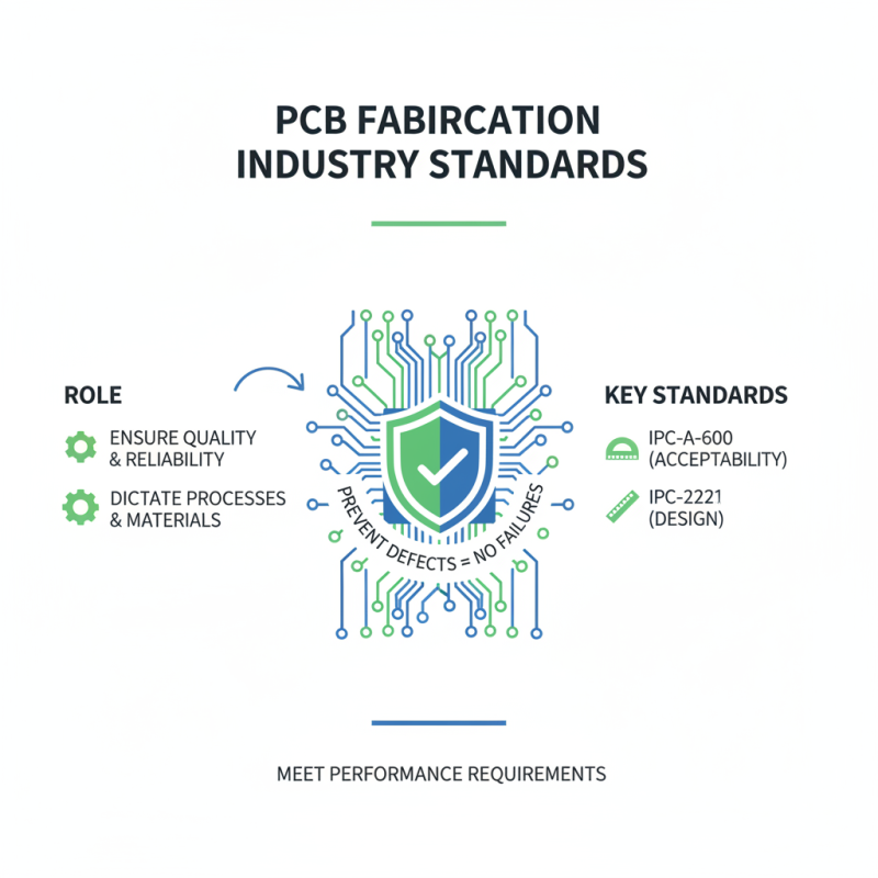
In PCB fabrication, industry standards play a crucial role in ensuring quality and reliability. These standards dictate the processes and materials used, making sure PCBs meet performance requirements. Common standards include IPC-A-600 for acceptability and IPC-2221 for design. Adhering to these standards helps prevent defects, which could lead to failures in electronic products.
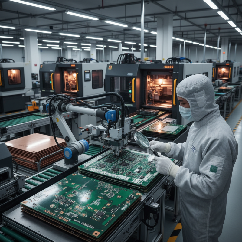
Quality control in PCB manufacturing involves several steps. Inspections occur at different stages, from raw material checks to final product testing. Automated optical inspection (AOI) is often employed to detect surface defects. Manual inspections still hold value, focusing on elements machines might miss.
Tips for improving PCB quality control:
1. Always verify incoming materials. Lower quality can compromise the final product.
2. Implement regular staff training to stay updated on industry standards. Knowledge helps in recognizing potential issues.
3. Create a feedback loop from the testing phase to continuously improve processes.
Every mistake in PCB manufacturing can be a learning opportunity. Reflect on failures and adjust practices accordingly. Continuous improvement is essential in this ever-evolving industry.
Future Trends in PCB Technology: Innovations and Challenges
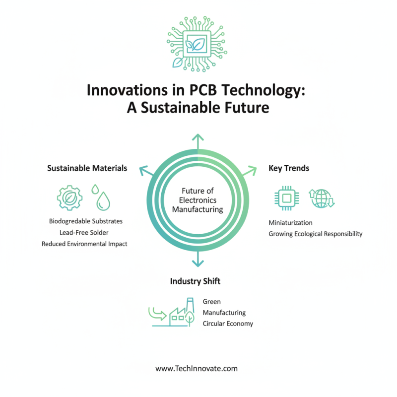
Innovations in PCB technology are rapidly shaping the future of electronics manufacturing. One trend is the shift toward more sustainable materials. Manufacturers are exploring options that reduce environmental impact. Biodegradable substrates and lead-free solder are gaining attention. These changes reflect a growing awareness of ecological responsibility.
Another notable trend is the miniaturization of PCBs. As devices get smaller, the components must fit into tighter spaces. This has led to advancements in design techniques and manufacturing processes. However, this miniaturization presents challenges. It can compromise signal integrity and thermal management if not executed properly. Engineers must navigate these obstacles carefully.
Lastly, integrating advanced technologies like AI and IoT is revolutionizing PCB design and production. Smart factories are emerging, where data-driven decisions improve efficiency. However, many companies face a knowledge gap in adopting these technologies. This creates a need for training and adaptation among workers. Balancing innovation with practical implementation is crucial for future growth in PCB manufacturing.