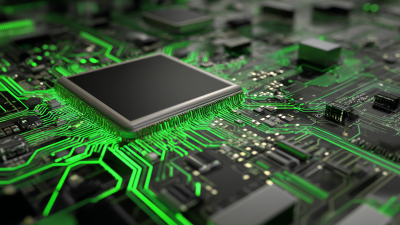
Why PCB Board Design is Crucial for Successful Electronic Projects
In the fast-evolving realm of electronics, the significance of PCB board design cannot be overstated. The global printed circuit board (PCB) market is projected to reach $101 billion by 2025, growing at a CAGR of 4.7% from 2020 to 2025, according to a report by Market Research Future. As electronic devices become increasingly sophisticated, the demand for reliable and efficient PCB designs intensifies. Renowned expert Dr. Emily Chen, a leading figure in electronic engineering, emphasizes that "the intricacies of PCB board design directly influence the functionality and longevity of electronic projects."
The process of PCB board design is not just a technical requirement; it is a critical factor that can determine the success or failure of an electronic project. A well-designed PCB can enhance signal integrity, reduce electromagnetic interference, and improve overall performance. Conversely, improper design can lead to significant issues, including device malfunction and increased production costs. As highlighted by a survey conducted by IPC – Association Connecting Electronics Industries, nearly 30% of electronic project failures can be traced back to inadequate PCB board design. This statistic underscores the pressing need for high-quality design practices in the industry.
As projects become more complex, the need for advanced PCB board design skills continues to rise. Designers must navigate factors such as miniaturization, thermal management, and material selection to deliver optimal results. In this landscape, investing in superior PCB board design is not merely advantageous but essential for any organization aiming for competitive differentiation and operational excellence.

Importance of PCB Board Design in Electronic Projects
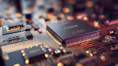
The design of a printed circuit board (PCB) is a fundamental aspect of any electronic project, influencing functionality, performance, and manufacturability. A well-crafted PCB layout ensures that all components are optimally placed for electrical efficiency and thermal management, reducing the risk of circuit failure. A flawed design can lead to signal integrity issues, unpredictable behavior, or even complete malfunctions, which may incur significant costs and delays in development.
Tips: When starting a PCB design project, always prioritize the creation of a comprehensive schematic. This serves as the blueprint for your layout, helping to prevent errors and streamlining the design process. Additionally, consider the physical dimensions of your device early on; a PCB that doesn’t fit the intended enclosure can cause unnecessary rework and complications.
Another important aspect of PCB board design is the consideration of manufacturing capabilities. Collaborate closely with your fabrication partner to understand their specifications and limitations. Doing so can help you choose appropriate pad sizes, trace widths, and hole diameters that adhere to manufacturing tolerances, ensuring a smoother production process. By paying attention to these details, you can enhance the overall reliability and performance of your electronic projects.
Importance of PCB Board Design in Electronic Projects
Key Principles of Effective PCB Design
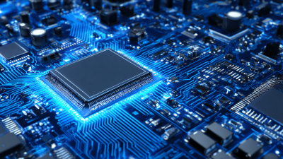
Effective PCB design is fundamental to the success of any electronic project. One key principle is the importance of a well-organized layout. A clean layout minimizes the chances of electromagnetic interference, which can adversely affect circuit performance. To achieve this, designers must prioritize component placement. Critical components should be positioned close together to reduce trace lengths, while maintaining sufficient space to prevent overheating and facilitate signal integrity. Additionally, incorporating grounding and power distribution planes effectively ensures that voltage levels are stable and consistent throughout the board.
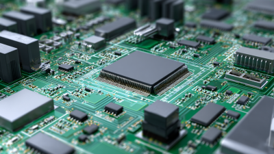
Another essential aspect of PCB design is understanding the thermal management of components. Heat dissipation plays a vital role in the longevity and reliability of electronic devices. Designers should assess the heat generated by components and choose appropriate techniques such as thermal vias, heat sinks, or adequate spacing between high-power components. Proper routing of traces is equally important; keeping high-speed signals short and avoiding sharp bends can help minimize signal loss and distortion. By adhering to these principles, engineers can create PCBs that not only function effectively but also support the overall objectives of the electronic project.
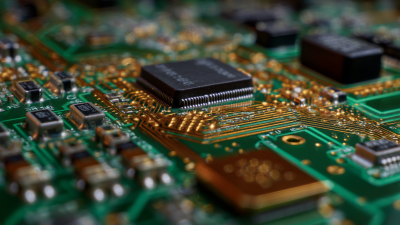
Impact of PCB Layout on Circuit Performance
The layout of a printed circuit board (PCB) is a critical element that directly influences the performance of electronic circuits. According to a recent industry report, nearly 70% of electronic project failures can be traced back to poor PCB design and layout choices. Effective PCB layout minimizes signal integrity issues such as crosstalk, reduces electromagnetic interference (EMI), and maintains proper impedance, ensuring that the circuit performs optimally at its intended frequencies. Additionally, a well-structured layout allows for better thermal management, which is crucial for maintaining the longevity and reliability of electronic devices.
To enhance your PCB layout, consider incorporating these essential tips:
- Utilize Ground Planes: Implementing a solid ground plane can significantly reduce noise and improve signal integrity, especially in high-frequency applications.
- Optimize Trace Width: Make certain to calculate trace width based on current requirements to prevent overheating and ensure efficient power distribution across the circuit.
- Minimize Loop Area: Keep your loop areas small to reduce inductance, thereby enhancing circuit performance and stability.
Investing time in meticulous PCB design will ultimately yield not just better performance but also increased efficiency and reliability in your electronic projects.
Common Challenges in PCB Board Design
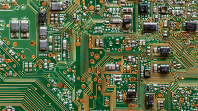
When delving into the nuances of PCB board design, one cannot overlook the common challenges that can arise during the process. One significant issue is the complexity of circuit layouts, which can lead to unintended design errors or signal integrity problems. As circuits become more intricate, ensuring that traces are adequately spaced and components are correctly oriented becomes pivotal. Overcrowding can result in noise interference and undesired crosstalk, which can dramatically affect the performance of the final electronic product.
Another challenge stems from the manufacturing capabilities and limitations. Designers must have a thorough understanding of the fabrication processes to avoid issues such as vias and pads being too small to be effectively produced. Additionally, ensuring thermal management is crucial, as insufficient heat dissipation can lead to component failure. Balancing the electrical performance with practical manufacturability requires a meticulous approach, making it vital for PCB designers to stay updated with the latest technologies and materials available in the industry. By addressing these challenges during the design phase, the chances of creating a successful electronic project are greatly enhanced.
Best Practices for Optimizing PCB Design Efficiency
The efficiency of PCB (Printed Circuit Board) design significantly impacts the overall success of electronic projects. According to a report by IDC, companies that implement best practices in PCB design can decrease their time-to-market by as much as 30%. This streamlining not only enhances product development timelines but also fosters innovation, enabling teams to focus on advanced functionalities rather than grappling with design inefficiencies.
One of the best practices to optimize PCB design is employing advanced simulation tools early in the design phase. These tools help engineers identify potential issues before they escalate into costly revisions. Furthermore, utilizing a modular design approach can enhance reusability across various projects, reducing the design time for new boards. A study by the IPC found that adopting these methodologies can lead to an average reduction of 25% in design-related issues during manufacturing.
**Tips:** Focus on clear documentation throughout the design process to ensure that any team member can understand and modify the PCB design later. Additionally, prioritize good communication among team members, which can significantly reduce misunderstandings and lead to a more cohesive product development experience.