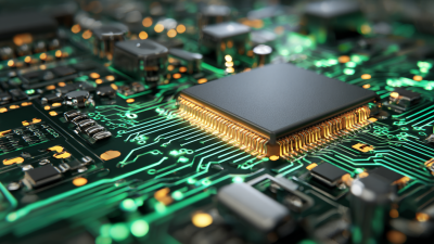
2025 How to Optimize Your PCB Board Assembly Process for Maximum Efficiency
In the rapidly evolving world of electronics, optimizing the PCB board assembly process has become a critical focus for manufacturers aiming to enhance efficiency and reduce costs. As we approach 2025, understanding the latest trends and techniques in PCB board assembly can provide significant competitive advantages. This introductory overview will highlight the top five strategies that can be employed to streamline assembly operations, minimize waste, and improve overall production timelines.
With the increasing complexity of electronic devices and the demand for faster turnaround times, manufacturers must adopt innovative approaches to PCB board assembly. These strategies not only involve advanced technologies and automation but also emphasize the importance of quality control and resource management. By implementing the right best practices, organizations can achieve superior product quality while maximizing their operational efficiency. This article will explore the essential components of an optimized PCB board assembly process and offer actionable insights for manufacturers looking to stay ahead in the industry.
Understanding the Current Trends in PCB Board Assembly Technologies for 2025
In 2025, the landscape of PCB board assembly technologies is undergoing significant transformation, driven by advancements in automation, artificial intelligence, and sustainable practices. One of the most prominent trends is the integration of AI-driven inspection systems that enhance the quality control process. These systems utilize machine learning algorithms to identify defects in real-time, thereby reducing the incidence of errors and minimizing waste. This enhances not only the efficiency of the assembly process but also ensures higher product reliability.
Moreover, the adoption of flexible manufacturing systems is revolutionizing how PCB assemblies are produced. These systems allow for more adaptive configurations, accommodating smaller batch sizes and short lead times, which are increasingly demanded by a fast-paced market. As manufacturers seek to optimize their processes, the use of advanced materials, such as eco-friendly substrates and lead-free soldering technologies, is also gaining traction. This shift not only aligns with global sustainability goals but also caters to the increasing regulatory requirements regarding environmental impacts in the electronics industry. All these trends indicate a future where efficiency and sustainability go hand in hand in PCB board assembly processes.
Key Strategies for Streamlining the PCB Design Process to Enhance Efficiency

To enhance efficiency in the PCB design process, it is essential to adopt key strategies that streamline workflows. First, utilizing advanced software tools for design automation can significantly reduce manual errors and speed up the design phase. These tools enable designers to create more accurate layouts and simulate performance outcomes before moving to production. Integrating automated design verification processes helps identify issues early, saving both time and resources in the later stages of manufacturing.
Another crucial strategy involves fostering collaboration among cross-functional teams, including design engineers, manufacturing experts, and quality assurance personnel. By establishing a continuous feedback loop, teams can ensure that design specifications align with manufacturing capabilities. This collaboration not only leads to a more coherent design process but also enhances communication, enabling faster resolution of potential issues. Ultimately, these strategies contribute to maximizing efficiency, reducing turnaround times, and improving the overall quality of PCB assemblies.
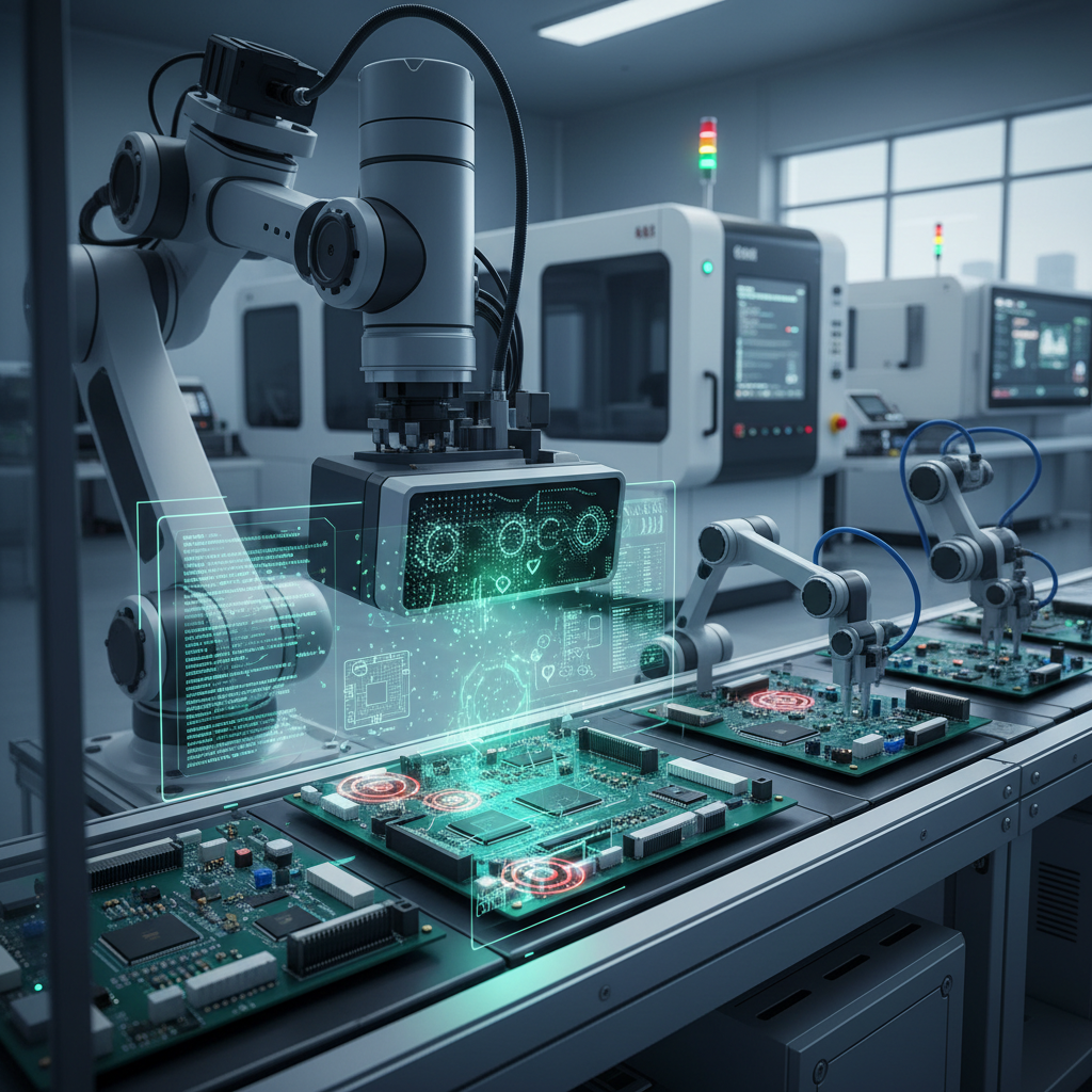
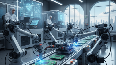
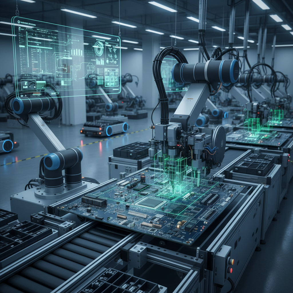
Implementing Automation Solutions in PCB Assembly for Optimal Workflow
Implementing automation solutions in PCB assembly is crucial for optimizing workflows and enhancing overall efficiency. By integrating advanced technologies such as robotic pick-and-place systems and automated optical inspection (AOI), manufacturers can significantly reduce the time and labor costs associated with manual processes. These automated systems not only streamline component placement but also ensure higher accuracy and quality control, minimizing errors that could lead to costly reworks.
Furthermore, incorporating software solutions such as Manufacturing Execution Systems (MES) allows for real-time monitoring and data analysis throughout the assembly process. This visibility enables manufacturers to identify bottlenecks quickly and adjust operations accordingly, ensuring smooth transitions from one phase of assembly to the next. Automation can also facilitate better inventory management, allowing for just-in-time manufacturing practices that enhance flexibility and responsiveness to market demands. By leveraging these technologies, PCB assembly can be transformed into a highly efficient and agile operation, poised to meet the challenges of a competitive industry landscape.
2025 PCB Board Assembly Process Optimization
The chart illustrates the reduction in assembly time as a function of the level of automation in the PCB assembly process. As companies implement automated solutions, the time required for assembly significantly decreases, leading to greater efficiency.
Best Practices for Quality Control in PCB Manufacturing to Minimize Errors
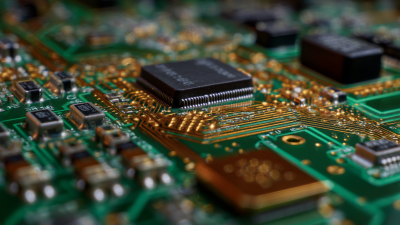
In the competitive landscape of PCB manufacturing, implementing rigorous quality control measures is essential for minimizing errors and ensuring product reliability. According to a report by IPC (Institute of Printed Circuits), as many as 40% of manufacturing defects originate from assembly processes. To counter this, adopting best practices in quality control can significantly enhance efficiency. For instance, integrating automated optical inspection (AOI) technology can detect defects in real-time, reducing the likelihood of faulty boards reaching the market.
Additionally, establishing a robust feedback loop between departments can further improve quality assurance. A survey by ResearchAndMarkets reveals that companies that actively engage in cross-functional collaboration experience a 30% reduction in production errors. By regularly reviewing assembly processes and implementing corrective actions based on data-driven insights, manufacturers can foster a culture of continuous improvement. These strategies not only enhance product quality but also contribute to operational efficiency, ultimately leading to higher customer satisfaction and loyalty in the PCB industry.
Future-Proofing Your PCB Assembly Operations: Sustainability and Cost-Effectiveness Strategies
As the demand for printed circuit boards (PCBs) continues to grow,
optimizing the assembly process for sustainability and
cost-effectiveness has become paramount. According to a report by IPC,
the global market for PCBs is expected to reach $82 billion by 2025,
emphasizing the need for manufacturers to adopt eco-friendly practices while maintaining profitability.
One effective strategy is to leverage automation and smart factory technologies,
which can significantly reduce waste and energy consumption. In fact, a study from the
International Society of Automation suggests that automating PCB assembly
can lead to a reduction in operational costs by up to 30%, making it an attractive option for
companies looking to future-proof their operations.
Additionally, integrating sustainable materials into the PCB assembly process can further enhance both
environmental impact and cost savings.
Research from the Electronics Industry Citizenship Coalition (EICC) indicates that
using recyclable materials and low-impact manufacturing techniques can decrease the carbon footprint
of PCB production by nearly 40%. By prioritizing materials that are environmentally friendly,
companies not only adhere to stricter regulations but also align with consumer preferences for sustainable products,
thereby improving brand reputation and customer loyalty in an increasingly eco-conscious market.
Embracing these strategies is essential for PCB manufacturers seeking long-term viability in a rapidly evolving industry.