Ultimate Guide to Printed PCB Design Tips and Best Practices for Beginners
The printed PCB (Printed Circuit Board) industry has rapidly evolved, becoming a cornerstone of modern electronics, facilitating innovations across various sectors such as health care, automotive, and telecommunications. According to a report by Market Research Future, the global PCB market is expected to reach USD 75 billion by 2026, growing at a CAGR of 4.65%. This surge indicates not only the increasing demand for sophisticated electronic devices but also the need for efficient and reliable PCB design practices among beginners entering this field.
Renowned PCB expert Dr. Emily Carter emphasizes the significance of proper design methodologies, stating, “A well-designed printed PCB is not just an accumulation of components; it is a synthesis of functionality, reliability, and manufacturability.” This insight underlines the importance of mastering design techniques and adhering to best practices for newcomers who aspire to create effective and compliant PCBs. This guide aims to provide essential tips and best practices, ensuring that beginners can navigate the complexities of printed PCB design with confidence and competence. Whether you are a hobbyist or an aspiring professional, understanding these fundamentals will pave the way for successful electronic project development.
Understanding the Basics of Printed Circuit Boards (PCBs)
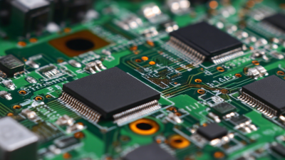
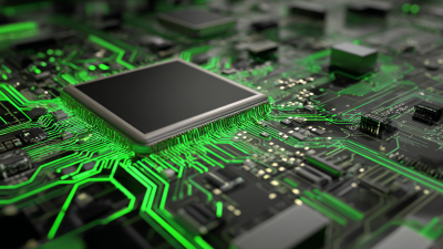
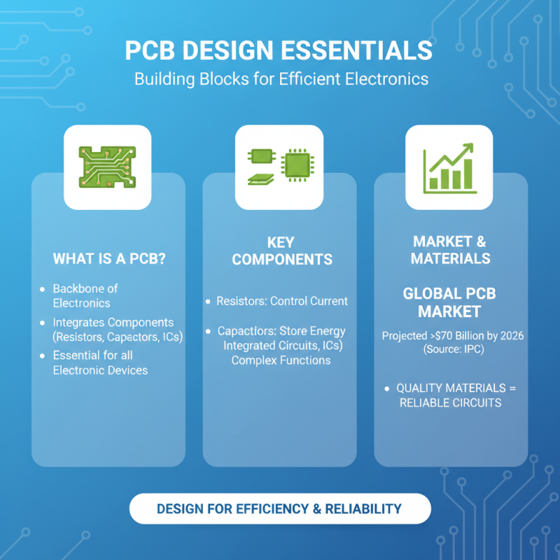
Understanding the basics of Printed Circuit Boards (PCBs) is essential for anyone venturing into the world of electronics. At its core, a PCB is a board made from insulating material that supports and connects electrical components. These components are typically attached to the PCB through a series of conductive pathways, allowing for efficient electrical flow. A fundamental aspect of PCB design involves understanding the layout, which dictates not only the placement of components but also their interconnections. This knowledge is crucial for reducing interference and ensuring optimal performance.
When embarking on PCB design, consider the following tips for success. First, always keep signal integrity in mind. This involves maintaining proper trace widths and lengths to minimize noise and interference. Additionally, use ground planes to enhance stability and reduce electromagnetic interference. Secondly, prioritize a structured approach in your design process. Utilizing software tools can streamline layout and enable simulation before fabrication. This proactive step helps identify potential issues early, saving time and resources.
Finally, ensure that your design is manufacturable by adhering to standard specifications. Familiarize yourself with design rules such as minimum trace widths and spacings, which can vary depending on the manufacturing capabilities. Meeting these criteria can significantly enhance the reliability of your final product and ease the transition from prototype to production. Understanding these foundational elements will not only improve your PCB design skills but also pave the way for more advanced techniques in the future.
Key Components and Materials Used in PCB Design
When embarking on PCB design, understanding the key components and materials is essential for creating efficient and reliable circuits. Printed Circuit Boards (PCBs) serve as the backbone of electronic devices, allowing for the integration of various components such as resistors, capacitors, and integrated circuits. According to a report by IPC, the global market for PCBs is projected to reach over $70 billion by 2026, highlighting the importance of quality materials in the industry.
Conductors, typically made of copper, are crucial as they facilitate electrical current flows. Their thickness and layout directly influence impedance, capacitance, and overall electrical performance of the PCB. Additionally, substrates like FR-4, a glass-reinforced epoxy laminate, offer mechanical strength and insulation. The selection of these materials can greatly affect thermal management and signal integrity in high-frequency applications, which are increasingly prevalent in modern electronics.
Solder mask and silkscreen materials also play a vital role in PCB design. Solder masks protect copper traces from oxidation and ensure proper soldering of components, while silkscreen provides necessary labeling for assembly and troubleshooting. As reported by research from the organization IPC, the demand for high-density interconnect (HDI) and flexible PCBs continues to rise, reflecting the industry's shift towards more compact and complex electronic designs that depend heavily on high-quality materials and components for optimal performance.
Essential Design Software for PCB Layout and Simulation
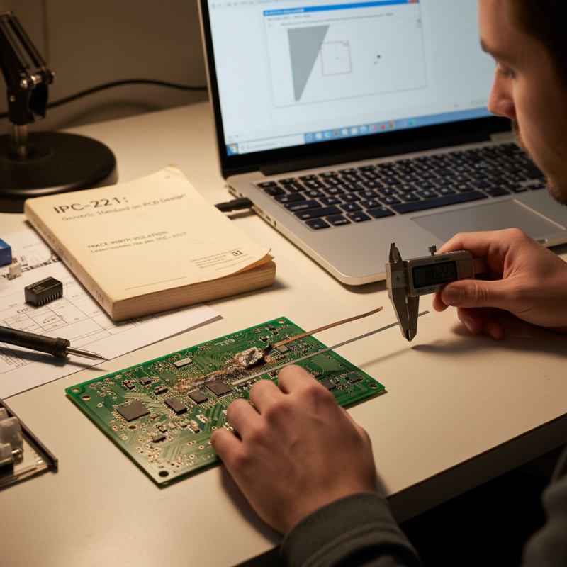
When it comes to printed circuit board (PCB) design, the choice of software is crucial for achieving efficient layouts and reliable simulations. According to a report by Research and Markets, the PCB design software market is projected to grow at a rate of over 8% annually, highlighting the increasing importance of advanced tools in electronics design. For beginners, selecting software that balances functionality and user-friendliness can significantly streamline the learning curve. Among the essential features to look for are schematic capture, design rule checking, and 3D visualization capabilities.
Moreover, simulation software plays a vital role in predicting how a PCB will perform under various conditions. A survey conducted by IPC found that nearly 75% of PCB designers believe that simulation tools reduce errors in the design process and help optimize layouts before manufacturing. This is particularly beneficial for new designers who might not yet have the experience to foresee potential issues.
Integrating simulation early in the design phase can lead to cost savings and a more efficient development cycle, as it allows for rapid prototyping and adjustments without the need for physical iterations. As the industry continues to evolve, embracing these essential design tools will be key to developing innovative and efficient PCB solutions.
Best Practices for PCB Layout and Routing Techniques
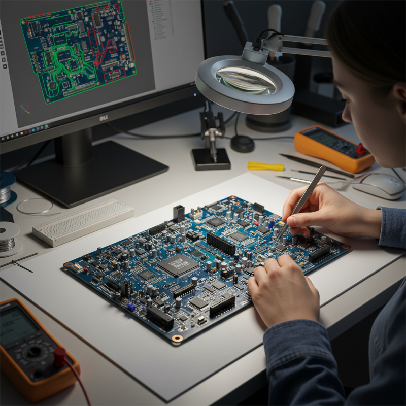
When it comes to PCB layout and routing, adhering to best practices is crucial for ensuring functionality, manufacturability, and reliability. One key principle is maintaining adequate spacing between traces, which reduces the risk of crosstalk and signal interference. According to a report from IPC, the Institute for Printed Circuits, nearly 22% of PCB failure is attributed to poor routing practices that lead to unintended short circuits and signal integrity issues. Thus, a minimum trace width of 0.2mm and a spacing of at least 0.2mm is recommended, especially in high-frequency designs.
Another essential aspect of PCB layout is the strategic placement of components. Grouping components that are electrically connected minimizes the length of traces needed and reduces inductive and capacitive effects. A study by the IEEE noted that optimal component placement could enhance the efficiency of signal transmission, improving performance by up to 30%. Additionally, implementing ground planes not only helps in shielding but also provides a low-resistance path for return currents, which is vital for the stability of the circuit. Overall, careful consideration of layout and routing techniques can significantly reduce design errors and enhance the overall performance and longevity of printed circuit boards.
Ultimate Guide to Printed PCB Design Tips and Best Practices for Beginners - Best Practices for PCB Layout and Routing Techniques
| Tip |
Description |
Best Practices |
| Keep It Simple |
Avoid unnecessary complexity in design. |
Focus on minimal component usage and fewer layers. |
| Proper Grounding |
Ensure a solid ground plane for better performance. |
Utilize a ground plane to reduce noise and improve signal integrity. |
| Trace Width Calculations |
Select appropriate trace widths to handle current loads. |
Use online calculators for accuracy based on current ratings. |
| Component Placement |
Strategically place components for efficient routing. |
Group related components together to minimize trace lengths. |
| Route Signals First |
Prioritize important signals during routing to ensure performance. |
Route high-frequency and sensitive signals first to reduce interference. |
| Minimize Via Usage |
Use vias sparingly to reduce signal loss. |
Limit the number of vias to improve reliability and signal integrity. |
| Design Rule Check (DRC) |
Utilize DRC tools to avoid errors during design. |
Run DRC frequently to catch potential issues early. |
Common Mistakes to Avoid in PCB Design for Beginners
When designing printed circuit boards (PCBs), beginners often fall into common pitfalls that can significantly affect the functionality and reliability of their projects. One of the most frequent mistakes is neglecting to check for proper trace width calculations. According to industry standards, using a trace width that is too narrow can lead to overheating and potential failure. Tools like IPC-2221 provide guidelines to help designers determine the right trace widths based on current-carrying requirements, ensuring safety and performance.
Another common error is overlooking the importance of grounding and power distribution. A well-designed PCB layout should include efficient ground planes and power distribution networks to minimize noise and enhance signal integrity. A report from PCB Design Magazine highlights that nearly 30% of PCB failures are related to poor grounding practices. Beginners should ensure that they understand concepts such as ground loops and the impact of return paths, which can greatly influence the overall performance of the circuit.
Finally, not planning for manufacturability can lead to costly revisions and delays. Designers often forget to consider fabrication tolerances, which can vary between manufacturers. According to a survey by Advanced Circuits, around 15% of PCB designs are rejected during fabrication due to issues that could have been avoided with proper planning. By adhering to design for manufacturability (DFM) principles and checking for compatibility with production capabilities early in the design process, beginners can streamline their PCB projects and avoid unnecessary setbacks.