10 Essential Tips for First Time PCB Manufacturing Success
In the rapidly evolving landscape of electronics, PCB manufacturing stands as a critical component that underpins the functionality and reliability of various devices. According to a report by Research and Markets, the global PCB market is projected to reach $75.2 billion by 2026, growing at a CAGR of 3.5% from 2021. This growth is driven by an increasing demand in sectors such as telecommunications, automotive, and consumer electronics. For first-time PCB manufacturers, navigating this complex environment can be daunting, which is why understanding essential best practices is crucial for success.

Dr. Emily Chen, a leading expert in electronic manufacturing and author of "Trends in PCB Manufacturing," emphasizes, “The key to success in PCB manufacturing lies not only in advanced technology but also in adhering to foundational best practices that minimize errors and maximize efficiency.” Her insights highlight the importance of strategic planning and thorough preparation for new entrants in the PCB manufacturing industry. By focusing on essential tips that encompass design, material selection, and quality control, novice manufacturers can mitigate risks and enhance their operational capabilities, setting a solid foundation for future growth in the competitive PCB landscape.
Understanding the Basics of PCB Manufacturing for Beginners
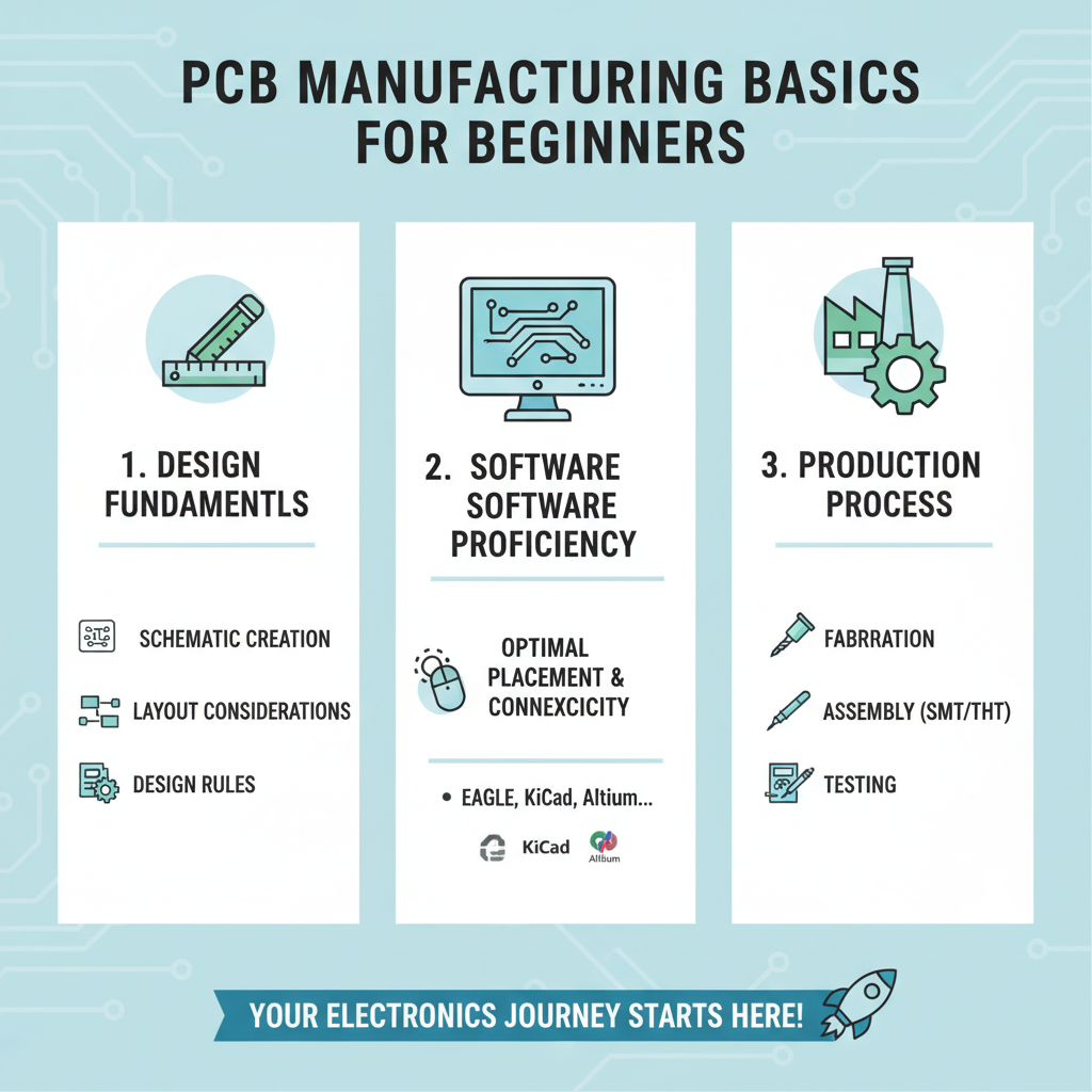
Understanding the basics of PCB manufacturing is crucial for beginners eager to dive into the electronics industry. A printed circuit board (PCB) serves as a foundation for electronic components, and grasping its design and production process can significantly impact project outcomes. Beginners should start by familiarizing themselves with the fundamental elements of PCB design, including schematic creation, layout considerations, and the importance of design rules. Knowing how to use PCB design software effectively can streamline the process, ensuring that all components are optimally placed and connected.
Another key aspect is selecting appropriate materials for the PCB. The choice of substrate, copper thickness, and solder mask can influence the board's functionality and durability. Beginners should also learn about the different manufacturing processes, such as etching and drilling, to understand how designs transition from computer to physical board. By engaging with online resources and seeking mentorship from experienced professionals, newcomers can build a solid foundation and avoid common pitfalls, ultimately paving the way for successful PCB manufacturing projects.
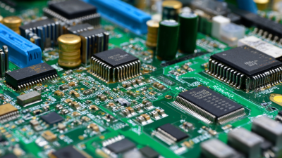
Choosing the Right Materials for Your First PCB Project
Choosing the right materials for your first PCB project is crucial to achieving success in PCB manufacturing. Recent industry reports indicate that approximately 20% of first-time PCB projects fail due to improper material selection. This emphasizes the importance of understanding the various materials available and their impact on performance, reliability, and cost. For example, FR-4 epoxy fiberglass is widely used in many PCBs for its excellent electrical insulation properties and thermal stability. However, alternative materials like polyimide can be advantageous for high-temperature applications where thermal resistance is necessary.
Moreover, the trend of hiding components within the PCB (referred to as "Oreo Construction") has gained traction among designers. This method not only enhances the aesthetic appeal of the board but also improves the overall space utilization. By incorporating built-in components, designers can create more compact and innovative designs, reflecting a shift in how PCBs are traditionally approached. As reported, projects utilizing this technique have reported up to a 30% reduction in footprint, allowing for more complex functionalities without the excessive size often associated with traditional layouts. Understanding these material properties and modern design trends can substantially elevate the quality and success rate of your PCB manufacturing endeavors.
10 Essential Tips for First Time PCB Manufacturing Success - Choosing the Right Materials for Your First PCB Project
| Tip Number |
Tip Description |
Material Considerations |
Recommended Thickness |
| 1 |
Understand Your Project Requirements |
Standard FR-4 |
1.6 mm |
| 2 |
Consider Environmental Factors |
FR-4 (with ENIG finish) |
1.6 mm |
| 3 |
Choose the Right Copper Weight |
Copper clad laminate |
1 oz |
| 4 |
Select Solder Mask Type |
Traditional green solder mask |
- |
| 5 |
Evaluate PCB Surface Finish Options |
HASL, ENIG, OSP |
- |
| 6 |
Understand the Importance of PCB Thickness |
FR-4 |
0.8 mm - 3.2 mm |
| 7 |
Investigate Mechanical Properties of Materials |
Thermal Performance of FR-4 |
- |
| 8 |
Prioritize Signal Integrity |
Low-loss materials |
- |
| 9 |
Plan for Heat Management |
Heat-resistant materials |
- |
| 10 |
Choose Cost-Effective Solutions |
Standard PCBs |
1.6 mm |
Design Considerations for Successful PCB Layouts
When embarking on your first PCB manufacturing project, design considerations are crucial for achieving a successful layout. Begin by understanding the purpose and functionality of your PCB. A well-defined schematic serves as the backbone of your design, ensuring that each component is accurately represented and connected. Paying close attention to the placement of components is essential; ensure that critical elements like power supply and grounding connections are positioned to minimize noise and interference.
Additionally, consider the design rules set by your PCB manufacturer. These rules often include minimum trace widths, spacing, and hole sizes, which are vital for ensuring manufacturability and reliability. Utilizing design software that incorporates DFM (Design for Manufacturing) guidelines can streamline this process, reducing the likelihood of costly errors.
Lastly, take the time to verify your design through simulations and prototype testing. This iterative approach not only enhances the performance of your PCB but also builds confidence before moving to full-scale production.
Testing and Validating Your PCB Before Production
Testing and validating your PCB before production is a crucial step that can save both time and resources in the manufacturing process. Before committing to a full production run, it’s essential to evaluate the design for functionality and reliability. Utilizing simulation software can help identify potential issues early on. By running various tests, such as signal integrity analysis, thermal performance assessment, and electrical testing, designers can ensure that the PCB will perform as expected in its intended application.
Once the initial tests are complete, creating a prototype is the next step. Fabricating a small batch of PCBs allows you to conduct real-world testing under actual conditions. This phase is vital for identifying unforeseen problems that simulations might not reveal. It’s advisable to gather feedback from stakeholders who will use or interact with the PCB, as their insights can highlight usability issues or design flaws. Thorough documentation of the testing results will be beneficial for refining the design and improving the overall quality before the final manufacturing process takes place.
PCB Manufacturing Success: Testing and Validation Metrics
Common Challenges in PCB Manufacturing and How to Overcome Them
Navigating the complexities of PCB manufacturing can be daunting for first-timers, but understanding common challenges can aid in the journey toward successful production. One prevalent issue is design errors, which often stem from inadequate knowledge of PCB design principles. To tackle this, investing time in thorough training and utilizing simulation tools can drastically reduce mistakes before production begins. Additionally, involving experienced engineers in the design phase can provide insights that can prevent costly errors later on.
Another challenge in PCB manufacturing is material selection. With a vast array of materials available, choosing the right one can be overwhelming. It's crucial to consider factors like thermal management and electrical performance based on the intended application. Establishing strong relationships with suppliers can help in gaining expert recommendations on material choices, minimizing trial-and-error in sourcing.
Lastly, effective communication with the manufacturing team is vital. Clearly conveying design specifications and tolerances helps mitigate misunderstandings that could lead to delays or defects, ultimately streamlining the entire PCB production process.