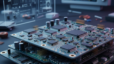
10 Essential Tips for Designing Printed Circuit Boards
In the world of electronics, designing a printed circuit board (PCB) is crucial. Experts like Dr. Emily Chen, a leading figure in PCB design, assert, “A well-designed PCB is the heart of any electronic device.” This statement underscores the importance of precision and thoughtfulness in the design process.
Designing a PCB goes beyond mere layout. Factors such as component placement, signal integrity, and thermal management all play significant roles. Small mistakes can lead to larger issues, such as failures in circuits. Even minor miscalculations in trace width can impact performance. Every detail counts in creating a reliable PCB.
Attention to detail is essential. It’s not just about aesthetics; it’s about functionality. For instance, ensuring correct spacing can avoid shorts and failures. Yet, designers often overlook these specifics, leading to regret later. A good PCB design requires creativity and technical knowledge. Balancing these elements is part of the challenge. Embracing this process can enhance both skill and final outcomes in the fast-evolving world of electronics.
Understanding the Basics of Printed Circuit Board (PCB) Design
When designing printed circuit boards (PCBs), understanding the basics is crucial. A PCB serves as the foundation for electronic circuits. It connects various components and enables functionality. Proper layout and routing are essential. Failure to consider these aspects can lead to significant issues, such as signal interference and connectivity problems.
Start with a clear schematic. This helps visualize the circuit’s flow. Use ground planes wisely. They reduce noise and improve performance. Pay attention to trace width. Thinner traces can overheat and fail, while wider traces can take up space unnecessarily. Don't ignore the importance of component placement. Cluttered designs can be hard to troubleshoot later.
Testing and revision are key steps. Prototypes often reveal flaws in design. A PCB that works on paper may not function correctly in reality. Be prepared for multiple iterations. Sometimes, minor adjustments can make a significant difference. A meticulous approach can lead to better results in the end, but it requires patience and frequent reflection on past mistakes.
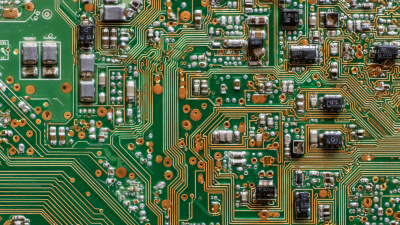
Selecting Appropriate PCB Materials for Optimal Performance
When designing printed circuit boards (PCBs), selecting the right materials can greatly influence performance. Materials such as FR-4 are popular due to their electrical and thermal properties. According to a 2022 IPC report, nearly 80% of PCBs are made from FR-4 due to its cost-effectiveness and reliability. However, not every application requires standard materials.
For high-frequency applications, materials like Rogers or Teflon can provide better performance. These materials minimize signal loss, crucial for 5G devices and satellite communications. In fact, studies show that using advanced materials can improve signal integrity by up to 30%. Yet, many designers overlook these specifications, focusing solely on budget.
Moreover, the thickness and layer counts affect overall board performance. Tighter tolerances can ensure functionality in compact designs. Yet, achieving such precision often increases production costs. A delicate balance between engineering and cost must be struck. Careful consideration of materials could save time and resources in the long run. Awareness of these nuances is essential for effective PCB design.
10 Essential Tips for Designing Printed Circuit Boards - Selecting Appropriate PCB Materials for Optimal Performance
| Material Type |
Dielectric Constant |
Thermal Conductivity (W/mK) |
Maximum Operating Temperature (°C) |
Cost ($/m²) |
| FR-4 |
4.6 |
0.3 |
130 |
10 |
| PTFE (Teflon) |
2.1 |
0.25 |
260 |
50 |
| CEM-1 |
4.3 |
0.25 |
130 |
8 |
| Polyimide |
3.5 |
0.5 |
400 |
80 |
| Rogers |
3.0-3.5 |
0.4 |
200 |
100 |
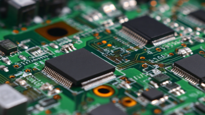
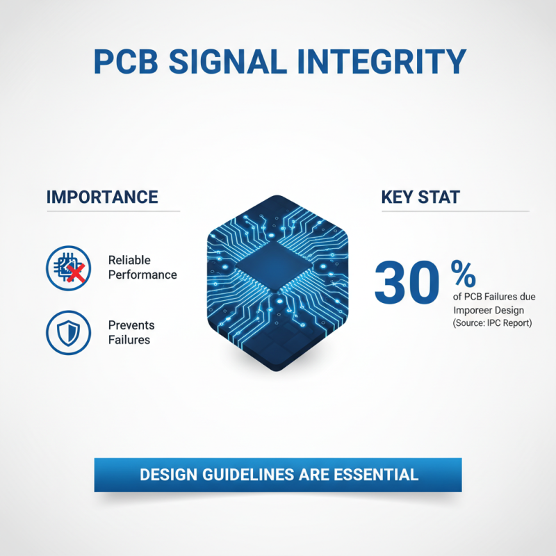
Essential Design Guidelines for Ensuring Signal Integrity
Designing printed circuit boards (PCBs) requires careful attention to signal integrity. Signal integrity is crucial for reliable performance in electronic devices. According to a report by IPC, improper design can lead to over 30% of PCB failures. This shows the importance of adhering to essential design guidelines.
One critical aspect is trace length and width. Shorter traces often yield better signal quality. In fact, a 1-inch trace can introduce significant delays. PCB designers should aim for trace widths that meet current capacity requirements and minimize resistance. Ground planes also play a vital role; they provide a return path for signals and reduce electromagnetic interference. However, many designs overlook the impact of ground layout.
Additionally, spacing between components should be thoughtfully planned. Too little space may cause crosstalk, while excessive spacing increases total area and costs. A staggering 70% of design errors stem from insufficient spacing. Measurements and simulations can guide effective design choices. Yet, many engineers still underestimate the power of simulation tools. They can save significant time and effort in the long run. Adjusting designs based on simulation findings leads to better quality products.
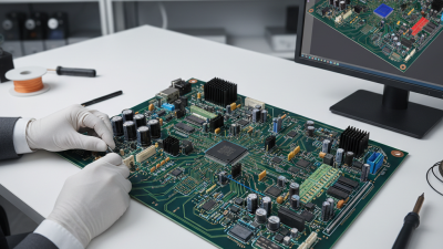
Best Practices for Testing and Debugging Your PCB Designs
Testing and debugging printed circuit board (PCB) designs is critical for ensuring functionality. A recent industry report stated that 30% of PCB failures can be traced back to design errors. Therefore, using a methodical approach is vital. Start by setting up a clear testing plan. Identify what aspects of the design can potentially fail. Visual inspection often reveals basic issues like soldering errors or component misplacement.
Simulating the expected environment is crucial for effective testing. Anomalies often surface when the PCB is subject to real-life conditions. For instance, temperature fluctuations can cause unexpected behavior. Use thermal cameras to detect hotspots during operation. Moreover, applying a systematic debugging process can save engineers time. Running through a checklist can help spot overlooked errors. According to research, up to 40% of debugging time is spent on issues that could have been caught earlier. Achieving a thorough documentation process is essential. It not only helps during the initial testing phase but also serves as a reference for future designs. The balance between extensive testing and time efficiency can be challenging. Detail-oriented engineers often find themselves trapped in exhaustive checks. Recognizing this pitfall is the first step toward improvement.
PCB Design Testing Efficiency by Phase