Electronic Contract Manufacturing Service Provider in California

10 Essential Tips for Designing a PCB Circuit Board Successfully

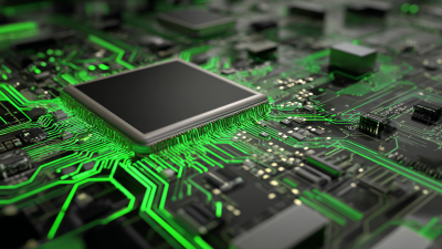
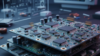
Designing a PCB circuit board is a fundamental step in the creation of electronic devices, serving as the backbone for various components to communicate effectively. As the complexity of technology continues to grow, the need for precision and efficiency in PCB circuit board design becomes increasingly critical. Whether you are a seasoned engineer or a beginner in the field, understanding the nuances of PCB design can lead to more successful outcomes and innovations.

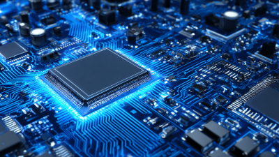
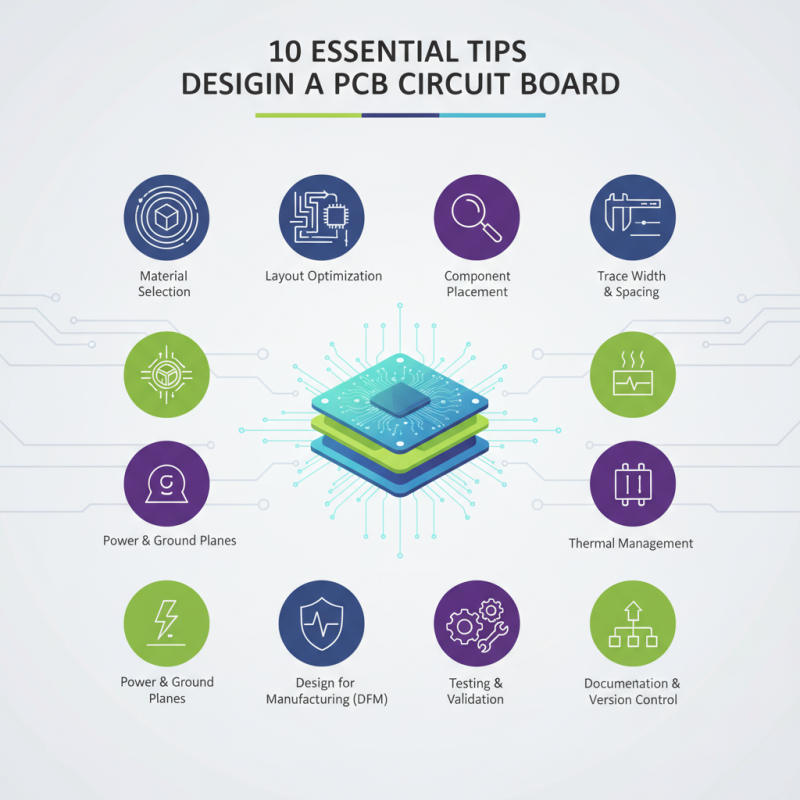
In this article, we will explore 10 essential tips that can enhance your PCB circuit board design process. From selecting appropriate materials to optimizing layout for maximum performance, each tip is aimed at ensuring reliability and functionality. Following these guidelines can help you avoid common pitfalls and streamline your design efforts, ultimately contributing to the success of your electronic projects. Join us as we delve into the key considerations and best practices that will empower you to design a PCB circuit board that meets industry standards and exceeds your expectations.

10 Essential Tips for Designing a PCB Circuit Board Successfully

Choosing the Right PCB Design Software for Your Project Needs

When embarking on a PCB design project, selecting the appropriate design software is critical to ensuring a smooth development process. Consider the specific requirements of your project, such as complexity, size, and design rules. For simple circuits, a user-friendly software option may suffice, while more intricate designs may necessitate advanced features such as multi-layer support and simulation capabilities. Evaluate the software's ability to handle the specific components and functionalities you need.

Another vital factor to consider is compatibility. Ensure that the software integrates well with the tools used for fabrication and testing. Additionally, assess the learning curve associated with the software; a steep learning curve could lead to delays in project timelines. Many design tools come with tutorials and support resources which can greatly assist beginners and streamline the design process. Ultimately, the right PCB design software can enhance productivity, facilitate easier collaboration within teams, and increase the chances of a successful project outcome.

Understanding the PCB Design Process: Key Phases Explained

The PCB design process consists of several critical phases, each of which plays a vital role in producing a functional and efficient circuit board. The journey typically begins with the conceptual design phase, where engineers determine the specifications and requirements of the PCB based on the intended application. This stage involves defining parameters such as size, layer count, and electronic components needed. Effective communication between team members and stakeholders is essential during this phase to ensure that all design goals align with the project's objectives.

Once the concept is solidified, the next phase focuses on schematic capture, where the electrical connections between components are documented. Designers use specialized software to create a visual representation of the circuit, ensuring that all components are accurately linked. Following the schematic design, the layout phase takes place, where the actual arrangement of components on the board is planned. This includes considerations like trace routing, layer stacking, and ensuring proper spacing to prevent interference. Each of these steps is crucial for optimizing the board's performance and manufacturability, thus leading to a successful PCB design process.

Essential Design Rules: Ensuring Signal Integrity and Minimizing EMI

10 Essential Tips for Designing a PCB Circuit Board Successfully

When designing a PCB, ensuring signal integrity is crucial to overall performance. One of the key aspects of achieving this is maintaining proper trace widths and spacing. Wider traces can carry more current and reduce resistance, which is essential for preventing overheating in high-power applications. Additionally, keeping adequate spacing between traces minimizes the risk of crosstalk, where signals can inadvertently couple and interfere with one another. Implementing differential signaling for high-speed signals can also significantly improve signal integrity by providing a balanced transmission path.

Minimizing Electromagnetic Interference (EMI) is another vital consideration in PCB design. A well-designed ground plane acts as a shield against unwanted electromagnetic fields, while also providing a return path for signals, thus enhancing overall performance. Utilizing longer ground connections can help in stabilizing signals and reducing inductive effects. It is also advisable to implement proper routing techniques, such as avoiding sharp angles and ensuring that traces are kept short and directly linked to their respective components. By following these essential design rules, designers can create PCB layouts that ensure signal integrity and mitigate EMI, leading to high-performing electronic circuits.

Selecting Appropriate Materials: Impact on Cost and Performance

10 Essential Tips for Designing a PCB Circuit Board Successfully

When designing a PCB circuit board, selecting the appropriate materials is crucial for optimizing both cost and performance. Different materials used in PCB construction have distinct properties that can significantly influence the electrical characteristics, durability, and overall functionality of the board. For example, the choice of substrate material can affect signal integrity; materials with better dielectric properties can minimize signal loss and enhance the speed and efficiency of the circuitry. Additionally, high-frequency applications require materials that can withstand higher thermal and environmental stresses without degrading, which underscores the importance of material selection.

Moreover, the materials chosen for a PCB can directly impact production costs. While high-performance materials may offer superior functionality, they often come at a premium price. Balancing the need for performance with budget constraints is a key challenge for PCB designers. Using standard materials may reduce costs but could compromise performance in certain applications. Therefore, evaluating the specific requirements of the project and the operating environment is essential. By strategically selecting materials that meet both performance expectations and cost considerations, designers can create effective PCBs that align with the intended application and market demands.

Common Pitfalls in PCB Design: How to Avoid Costly Mistakes

When designing a PCB circuit board, avoiding common pitfalls is essential for ensuring both functionality and cost-effectiveness. One frequent mistake is neglecting to plan the layout in relation to component placement. This can lead to unwanted interference and signal integrity issues. To mitigate these risks, it's crucial to consider the routing paths of all connections early in the design phase. Use design software that allows for detailed visualizations to help identify potential conflicts before they become problematic.

Another common error is underestimating the importance of grounding and power distribution. Poorly designed ground planes can introduce noise and affect the overall performance of the board. Ensuring a robust grounding strategy can significantly enhance reliability. Additionally, using decoupling capacitors strategically can aid in minimizing voltage fluctuations that may arise from various components switching on and off.

A critical tip is to thoroughly review design rules and constraints before finalizing your PCB layout. This proactive approach can prevent issues related to component spacing, trace width, and thermal management. Utilizing simulation tools can also help detect design flaws early, potentially saving time and resources. By staying vigilant and methodical during the design process, you can create a successful PCB while minimizing costly mistakes that may arise from oversight.

10 Essential Tips for Designing a PCB Circuit Board Successfully - Common Pitfalls in PCB Design: How to Avoid Costly Mistakes

Tip Description Common Pitfall How to Avoid
1. Start with a Clear Design Specification Define the requirements and specifications for your PCB before starting the design process. Vague specifications lead to design flaws. Thoroughly document requirements and review them with stakeholders.
2. Choose the Right Materials Select appropriate substrate and components for your application's needs. Using subpar materials can lead to failures. Research and select high-quality materials that match your specifications.
3. Keep Traces Short and Thick Minimize trace length to reduce resistance and improve performance. Long, thin traces can cause signal integrity issues. Use wider traces for higher current and keep routing efficient.
4. Pay Attention to Grounding Ensure proper grounding to prevent interference and noise. Inadequate grounding can lead to erratic behavior. Use ground planes and minimize ground loops.
5. Use Design Software Effectively Utilize PCB design software features to streamline the design process. Ignoring software tools can lead to inefficiencies. Take advantage of tutorials and documentation to maximize tools.
6. Plan for Heat Dissipation Consider thermal management in your PCB design to avoid overheating. Overheating can damage components. Use heat sinks and proper layout techniques for airflow.
7. Prototyping and Testing Create prototypes and conduct rigorous testing to identify issues. Skipping prototypes can cost more in the long run. Invest in a development phase for troubleshooting.
8. Ensure Proper DFM and DFT Design for manufacturability and testability to simplify production. Neglecting DFM/DFT can lead to costly redesigns. Collaborate with manufacturers during the design phase.
9. Document Your Design Process Keep detailed records of your design decisions and changes. Lack of documentation can cause confusion later. Create a comprehensive design log throughout the project.
10. Stay Updated with Technology Trends Keep abreast of new technologies and methodologies in PCB design. Being outdated can hinder project effectiveness. Attend workshops, webinars, and industry conferences.