2026 How to Design PCB for Beginners and Professionals?
In the world of electronics, knowing how to design PCB is essential. Experts like John Doe, a seasoned PCB designer, emphasizes, "Good design is not just about creativity; it’s about functionality." Beginners and professionals alike face a myriad of challenges when embarking on PCB design. The balance between aesthetics and practicality is often tricky.
Many newcomers struggle with software tools, while seasoned professionals may find themselves stuck in outdated designs. The evolution of PCB technology demands continuous learning and adaptation. A well-designed PCB can be the difference between a successful product and a failure. It’s important to assess every element carefully, avoiding common pitfalls.
Errors can be costly and frustrating, especially when working on time-sensitive projects. Designers must reflect on their past mistakes. Each failure offers a lesson. In this journey, mastering the art of design PCB can be a rewarding experience, but it requires patience and diligence.

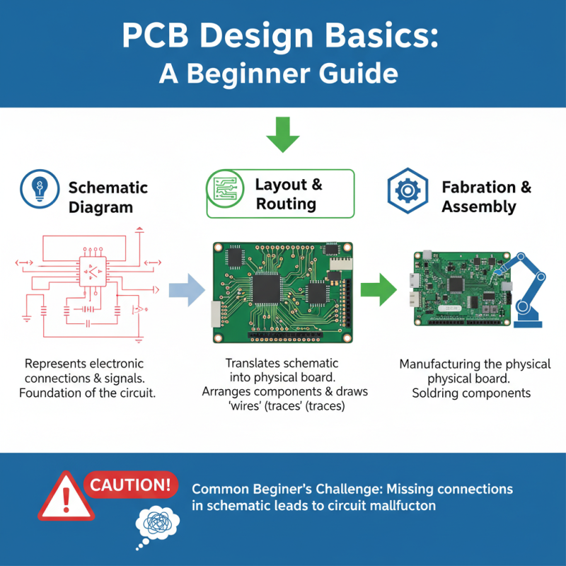
Understanding the Basics of PCB Design: A Beginner's Guide
PCB design can seem daunting, especially for beginners. Understanding the basic concepts is crucial. At its core, a PCB, or printed circuit board, connects various components in an electronic device. You start with a schematic diagram. It represents the connections and signals. This is where many beginners face challenges. They might miss important connections, leading to malfunctioning circuits.
Once the schematic is ready, you move on to layout design. Here, you place components on the board. It’s essential to consider the size and spacing. Cluttered designs can lead to interference. Additionally, route the traces carefully. They must connect the components without crowding. Mistakes can disrupt signals.
Finally, the design needs to be checked. Many overlook this step. Using simulation software can help identify issues. A PCB is an iterative process. Expect to revise your design multiple times. Learning from errors is part of the journey. Embrace the challenges; they will make you a better designer in the long run.
Essential Tools and Software for PCB Designers
When designing PCBs, choosing the right tools is crucial. A recent industry report highlights that about 75% of PCB designers prefer software that integrates simulation and layout features. This integration saves time and reduces errors. Popular software typically includes schematic capture and design rule checkers. These tools help beginners grasp fundamental concepts quickly.
For professionals, advanced simulation tools can enhance design capabilities. They allow for signal integrity analysis and thermal management assessments. According to a survey, over 60% of professional designers noted that these tools improved their productivity significantly. However, they also pointed out that mastering these tools can be challenging. Many experienced users still face a steep learning curve when adapting to new features.
Affordable open-source options are emerging, attracting beginners. Yet, the functionality might not rival expensive commercial tools. Users may struggle with limited support and resources. Choosing the right software requires a careful evaluation of project needs and personal expertise. Balancing budget constraints with necessary features can be complex, often leading to imperfect decisions.
Step-by-Step Process of Designing a PCB
Designing a PCB requires careful planning and execution. Knowing the fundamentals is crucial. Start with a clear schematic. This lays the groundwork for your layout. Use software to create your designs. Many tools are available, ranging from beginner-friendly to more complex options. Each tool has its quirks. Expect a learning curve, and don't rush through it.
Next, focus on the layout. Place components thoughtfully. Pay attention to trace widths and lengths. They influence performance and signal integrity. Avoid cluttering your board. A clean design is easier to debug. Mistakes are often made here. Remember to check your connections multiple times. Testing before final production is vital.
Finally, think about the manufacturing process. Specifications matter. Be aware that variations in material can impact your design. Some designs may fail to function as expected. Analyze your results critically. Learning from mistakes is part of growth in PCB design. Embrace the process, and continuously refine your skills.
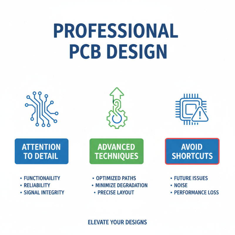
Advanced Techniques for Professional PCB Design
In professional PCB design, attention to detail is crucial. Advanced techniques elevate the functionality and reliability of your designs. For example, considering the layout of traces is not just about aesthetics. Optimizing the path length can minimize signal degradation. Tight spaces may tempt shortcuts, but this often leads to future issues.
Utilizing software tools effectively can enhance your design process. Features like DRC (Design Rule Check) are vital. They help catch errors early, saving time and resources. However, don't rely solely on tools. Manual inspection remains important. A fresh set of eyes can identify potential problems that software may overlook.
Thermal management is another area to consider seriously. Components generate heat, which can affect performance. Adequate spacing and heat sinks can mitigate risks. However, many overlook this until it becomes a critical issue. Be proactive in your approach to avoid costly mistakes down the road.
Common Mistakes to Avoid in PCB Design Projects
In PCB design, avoiding common mistakes is crucial for success. One prevalent error is neglecting to ensure adequate trace width. According to a report by IPC, over 30% of PCB failures stem from inadequate trace sizing. A trace that's too narrow can lead to overheating and eventual failure. Always consult the IPC-2221 standards for guidance on trace width versus current capacity.
Another frequent pitfall involves improper component placement. Designers often overlook the thermal performance of specific components. A misplaced component can hinder heat dissipation, leading to potential circuit failure. Research indicates that about 40% of design flaws arise from incorrect layout and placement. Pay close attention to the power distribution network to prevent issues.
Additionally, underestimating the importance of a ground plane can be detrimental. A robust ground plane enhances signal integrity and reduces electromagnetic interference. However, many designs ignore this aspect, resulting in compromised performance. Ensure the ground plane is continuous and unbroken to minimize noise. Remember that these mistakes, while common, can be avoided with careful planning and attention to detail.