How to Choose the Right PCB Fabrication Process for Your Project
Choosing the right PCB fabrication process is a crucial step in ensuring the success of any electronic project. The complexity and specifics of the project can greatly influence which fabrication method will yield the best results. In the realm of PCB fabrication, various methods offer unique advantages and challenges that must be carefully considered. From rapid prototyping to mass production, each technique serves a distinct purpose and is suited for different application needs.
This guide delves into the essential factors to consider when selecting a PCB fabrication process. Understanding the technical requirements, budget constraints, and timeline for your project can help streamline the decision-making process. By exploring the intricacies of different fabrication techniques, you can align them with your project goals, whether you're developing a simple circuit board or an intricate multilayer design. Ultimately, the right PCB fabrication process can enhance reliability, optimize performance, and elevate the overall quality of your electronic products.
Understanding PCB Fabrication Processes: An Overview of Types and Technologies
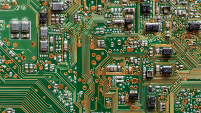
Choosing the right PCB fabrication process for your project requires a comprehensive understanding of the various types and technologies available in the market. The main fabrication processes can be categorized into several key types, including subtractive, additive, and hybrid technologies. Subtractive processes, which include traditional etching techniques, account for approximately 80% of the PCB fabrication industry, as reported by industry analysts. These methods are ideal for high-volume production due to their cost-effectiveness and efficiency. On the other hand, additive processes, which are instrumental in building 3D structures layer by layer, are gaining traction, especially for prototypes and specialized applications. According to a report by IPC, additive manufacturing in PCB fabrication is expected to grow by 30% over the next five years.
When selecting a fabrication process, it is crucial to consider factors such as design complexity, material requirements, and production volume. For example, if your project involves intricate designs or smaller quantities, it may be beneficial to leverage additive technologies. Conversely, for mass production where standardization is key, subtractive techniques remain the preferred choice.
**Tips:** Always evaluate the most recent trends in PCB technologies, as advancements such as automated manufacturing systems and advanced material applications can significantly impact your project’s outcome. Engaging with industry experts or utilizing simulation software can also help optimize your design for the selected fabrication process, ensuring a seamless transition from concept to production.
How to Choose the Right PCB Fabrication Process for Your Project
| Fabrication Process |
Description |
Key Advantages |
Best Use Cases |
| Conventional PCB Fabrication |
Standard process using etching to create circuit patterns. |
Cost-effective for medium to large volume runs. |
Consumer electronics, appliances. |
| HDI PCB Fabrication |
High-Density Interconnector Boards with finer lines. |
Allows for more functionality in smaller form factors. |
Mobile devices, IoT applications. |
| Flexible PCB Fabrication |
Printed circuit boards that can bend and flex. |
Ideal for compact and lightweight designs. |
Wearable technology, medical devices. |
| Rigid-Flex PCB Fabrication |
Combines rigid and flexible circuits into one assembly. |
Reduces weight and enhances design possibilities. |
Aerospace, military applications. |
| Multi-layer PCB Fabrication |
PCBs with more than two conductive layers stacked together. |
Increases circuit density without enlarging the board size. |
High-performance computing, telecommunications. |
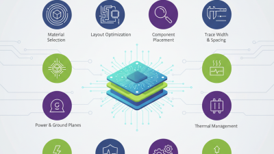
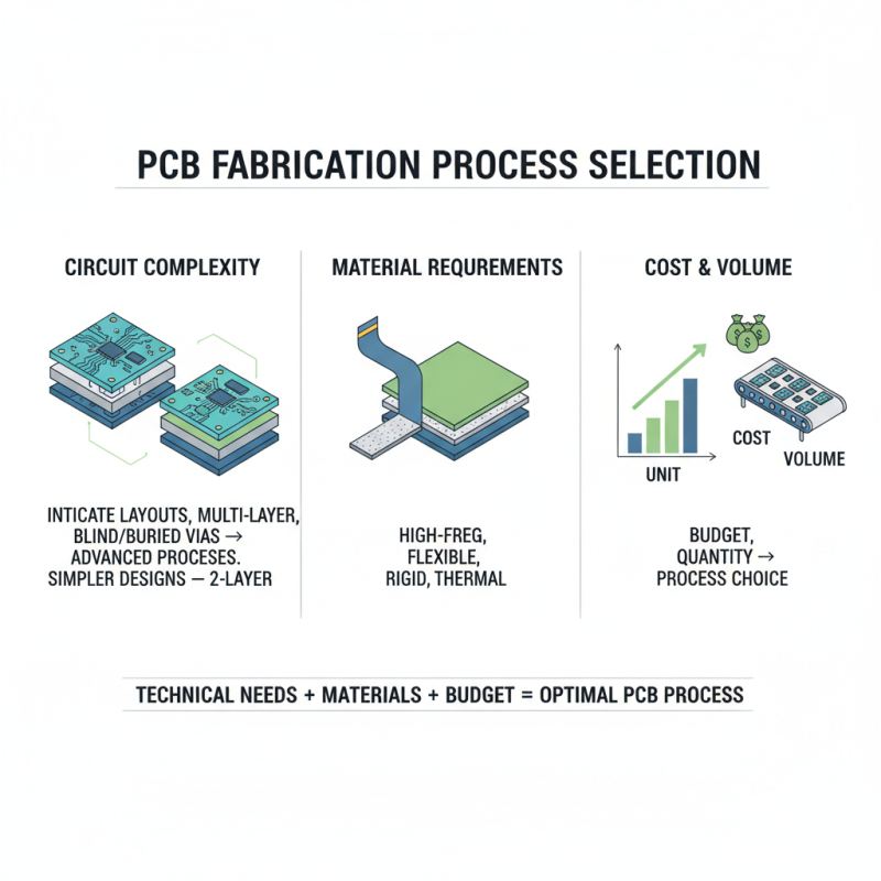
Key Factors Influencing PCB Fabrication Process Selection
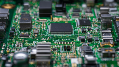
When selecting a PCB fabrication process, several key factors come into play that can influence the success of your project. Firstly, the complexity of the circuit design is paramount. If your PCB requires intricate layouts, multiple layers, or advanced technologies like blind and buried vias, choosing a process capable of handling these complications is essential. For instance, multilayer PCB fabrication may be necessary for high-density interconnect designs, whereas simpler applications might suffice with two-layer options. Understanding the technical requirements of your design helps narrow down suitable fabrication processes.
Material selection is another critical factor. Different PCB materials offer varying properties such as thermal management, electrical insulation, and mechanical strength, which can significantly impact performance. For example, high-frequency applications might benefit from materials specifically engineered for low-loss characteristics, while rugged environments might necessitate sturdier substrates. Ultimately, aligning the material choice with the operational demands of the final product ensures reliability and efficiency. Additionally, cost considerations and production timelines can further guide your decision, as balancing performance with budget constraints is crucial for successful project execution.
Comparative Analysis of Cost-Effectiveness in PCB Manufacturing Methods
When evaluating the cost-effectiveness of various PCB manufacturing methods, it is crucial to understand the intricacies of each process. Traditional methods such as subtractive manufacturing, while widely used, can lead to higher material waste and longer production times. By utilizing recent advancements in additive manufacturing, companies can minimize waste and optimize material usage, which ultimately drives down costs. This method allows for greater design freedom and flexibility, making it a compelling option for prototypes or low-volume production runs where cost sensitivity is paramount.
Additionally, the choice between manual and automated production processes can significantly impact overall expenses. Manual assembly tends to require a higher labor input, which can lead to increased costs if economies of scale are not achieved. Conversely, automated processes tend to be more efficient, particularly for large volume productions, where the initial investment in machinery is offset by reduced labor costs and improved consistency. Therefore, a detailed analysis of the project requirements—including expected volumes, design complexity, and budget constraints—is essential for selecting the most cost-effective PCB fabrication method that aligns with your project's goals.
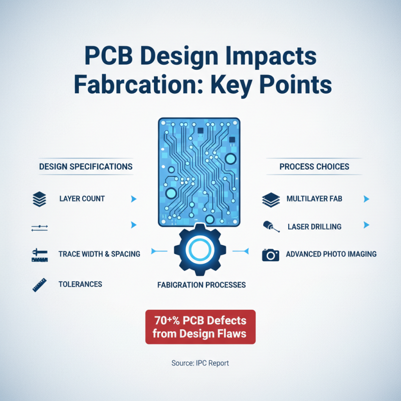
Impact of Design Specifications on PCB Fabrication Choices
The design specifications of a printed circuit board (PCB) significantly influence the choice of fabrication processes, as they dictate the technical requirements and capabilities necessary for successful manufacturing. A report by IPC, the global trade association for the electronics industry, highlights that over 70% of PCB defects stem from design flaws, underscoring the need for precise specifications. For instance, decisions around layer count, trace width, and spacing directly affect the choice of manufacturing techniques. Higher layer counts may necessitate advanced processes like multilayer PCB fabrication, while tighter tolerances might require precision techniques such as laser drilling and advanced photo imaging.
Furthermore, the complexity of the design also plays a crucial role in the choice of the fabrication method. According to industry analysis by Market Research Future, the global demand for flexible PCBs is expected to grow at a CAGR of around 14% from 2021 to 2027, driven by designs that integrate flexibility into electronic devices. Fabricators must consider the material properties, such as thermal and electrical performance, as well as the intended application when selecting the appropriate fabrication process. For example, substantiating a design that requires high thermal conductivity might lead to the use of specialized copper plating techniques, while a design aimed at miniaturization may prioritize high-density interconnect (HDI) fabrication methods. Ultimately, aligning design specifications with the right PCB fabrication process is crucial for achieving the desired performance and reliability in electronic applications.
Future Trends in PCB Fabrication: Innovations and Industry Standards
The future of PCB fabrication is poised for significant transformation, driven by technological innovations and evolving industry standards. Recent reports indicate that the global printed circuit board market is projected to reach approximately $80 billion by 2026, highlighting an increased demand for advanced manufacturing techniques. Innovations such as additive manufacturing and high-density interconnect (HDI) technology are shaping the way PCBs are designed and produced, enabling the creation of more compact and efficient electronic devices.
Additionally, industry standards continue to evolve in response to the growing complexity of electronic assemblies. The implementation of Industry 4.0 practices, which include automation, data exchange, and smart manufacturing, is becoming increasingly prevalent in the PCB fabrication sector. According to a study by IPC, over 76% of manufacturers are actively integrating automation within their processes to enhance production efficiency and reduce lead times. Moreover, developments in sustainable materials and processes are gaining traction, as environmental regulations exert pressure on manufacturers to adopt greener practices. Such advancements not only optimize production but also align with global sustainability goals, making them critical for future-proofing PCB fabrication projects.
PCB Fabrication Process Adoption Trends (2023)