Best PCB Fab Techniques for High Quality Manufacturing?
In the rapidly evolving world of electronics, high-quality PCB fab techniques are crucial. The demand for advanced printed circuit boards has surged. According to a recent market report by IPC, the global PCB industry was valued at approximately $60 billion in 2022, with an expected growth rate of 3.5% annually. This upward trend signifies the increasing complexities in manufacturing processes.
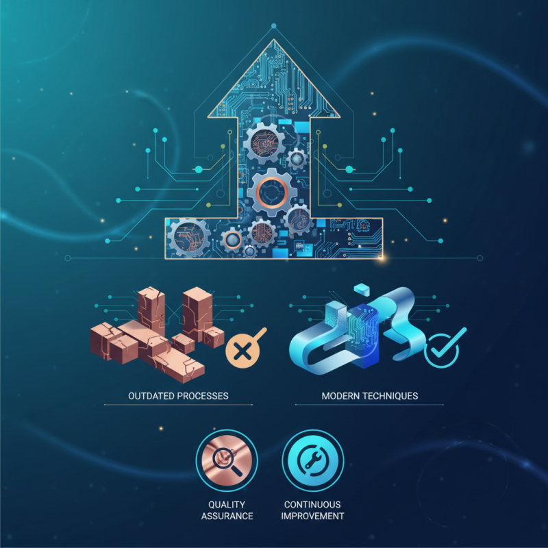
Experts highlight the importance of precision in PCB fab. Dr. Robert Cheng, a well-known figure in the industry, asserts, "Quality in PCB fabrication is non-negotiable for reliable electronic devices." Many manufacturers struggle to achieve this quality consistently. Issues often arise from outdated processes or insufficient quality control measures.
Investing in modern techniques is essential. Techniques such as laser cutting and advanced surface finish processes can significantly improve outcomes. Yet, mistakes can still occur. Quality assurance should always be a priority. Continuous improvement practices help address flaws. Recognizing where improvements can be made is vital for success in PCB fab.
Understanding the Basics of PCB Fabrication Techniques
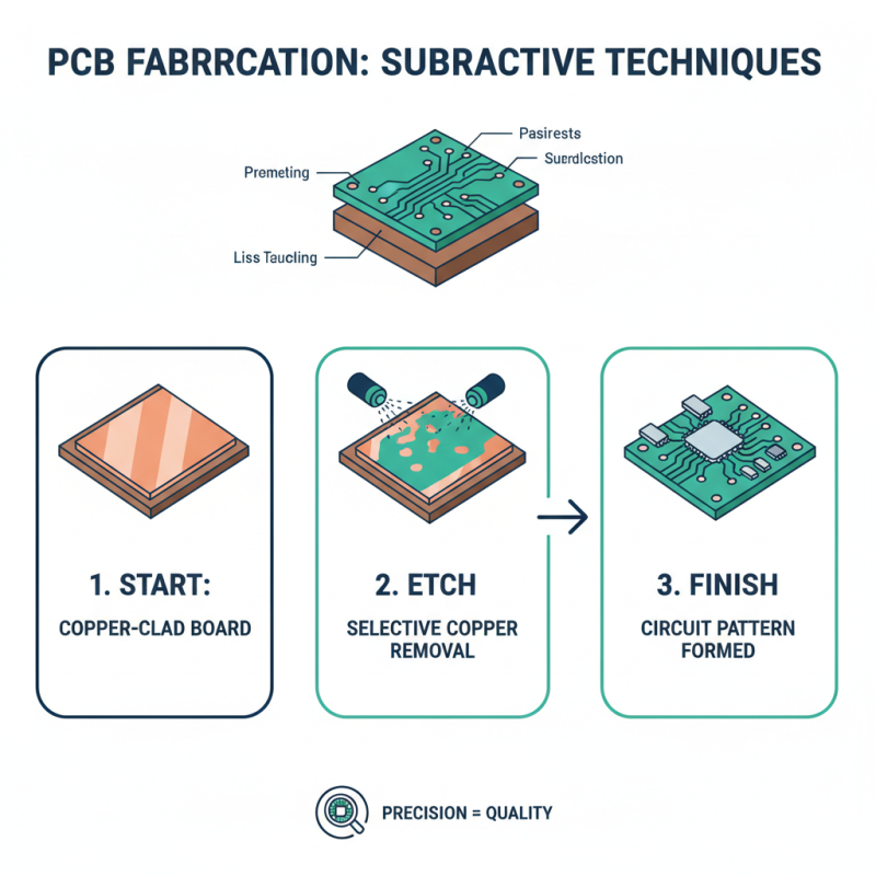
PCB fabrication is a crucial process in electronics manufacturing. Understanding the basics of these techniques is vital for achieving high quality in production. The most common method involves subtractive techniques, which start with a copper-clad board. In this process, layers of copper are removed to create the desired circuit pattern. Precision is key here, as any errors can lead to inefficient designs.
Another technique worth exploring is additive manufacturing. This method builds up the circuit layer by layer, allowing for complex designs. While it offers flexibility, it can be challenging to ensure uniformity. Sometimes, the layers do not adhere properly, leading to defected circuits. This requires constant monitoring and adjustments.
A less common approach is hybrid manufacturing, which combines subtractive and additive techniques. While it provides unique solutions, it can also introduce complexity. Designers must stay alert to potential issues during integration. A thorough understanding of these basics helps ensure durable and effective PCB designs, though it's essential to monitor each step closely.
Key Factors Influencing PCB Quality in Manufacturing
When manufacturing printed circuit boards (PCBs), several key factors influence the overall quality. Material selection is critical. High-quality raw materials lead to better performance and longevity. According to industry reports, using premium copper and robust dielectric materials can reduce defects by up to 30%. This is significant in ensuring the reliability of electronic devices.
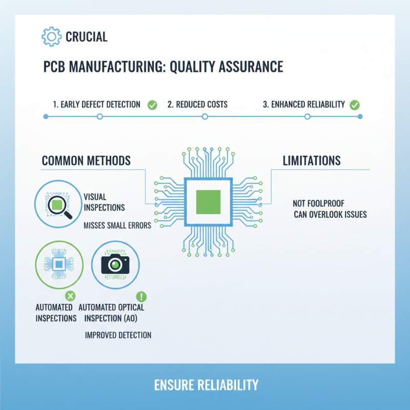
Another important aspect is the precision of the fabrication process. Tolerances must be tightly controlled. A recent study found that PCB designs with clear specifications reduced production errors by 25%. However, many manufacturers still struggle with inconsistencies, often leading to reworks. Inspection techniques also matter. Automated optical inspection (AOI) systems can detect flaws quickly, but they are sometimes bypassed, risking quality.
Environmental conditions during manufacturing can impact outcomes too. Humidity and temperature control are often overlooked, yet they can affect solder adhesion and trace integrity. Research indicates that 15% of defects are linked to improper environmental management. These nuances reveal that PCB fabrication is complex. Each element must be meticulously managed to produce high-quality boards.
Best PCB Fab Techniques for High Quality Manufacturing - Key Factors Influencing PCB Quality in Manufacturing
| Technique |
Description |
Key Benefits |
Impact on Quality |
| Controlled Impedance |
Maintaining consistent impedance throughout the PCB to ensure signal integrity. |
Improved signal performance and reliability. |
Minimizes signal distortion and reduces EMI. |
| Layer Stackup Optimization |
Designing the arrangement of layers to reduce fabrication costs and enhance performance. |
Cost-effective and high-performance boards. |
Enhances thermal management and electrical performance. |
| High-Density Interconnect (HDI) |
Utilizing microvias and finer traces for complex circuit designs. |
Increased routing density and smaller form factor. |
Allows for more functionalities in a compact space. |
| Surface Finish Selection |
Choosing appropriate surface finishes like ENIG or OSP for soldering compatibility. |
Enhanced solderability and longevity. |
Reduces oxidation and improves the solder joint quality. |
| Via Fill and Plating |
Filling vias with conductive materials to improve thermal and electrical conductivity. |
Better thermal performance and reliability. |
Reduces the risk of voids in solder joints. |
Advanced PCB Fabrication Methods for Precision Engineering
Advanced PCB fabrication methods are essential for
precision engineering. These techniques enhance the performance and
reliability of printed circuit boards. One popular method is laser drilling.
This allows for smaller holes with better accuracy. Laser technology reduces the risk of damage during production,
which can be a common issue.
Another technique involves using advanced photoresists. These materials improve
the fidelity of patterns on PCBs. However, the application process can be tricky. If not done correctly, the final
results may not meet expectations. Inconsistent exposure times can lead to defects
in the board layout. Precision is vital, but even small errors can have significant impacts.
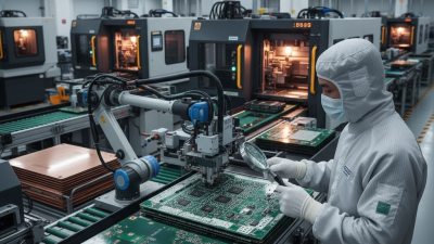
Surface mount technology (SMT) is also crucial for modern
PCBs. SMT enables compact designs and can handle high-density components. Yet, this method requires meticulous
attention. Suboptimal placement can result in connectivity issues. Engineers must continually refine their methods.
Each iteration brings new challenges that need addressing for better outcomes.
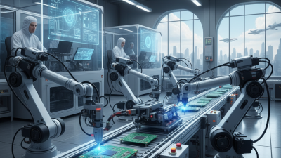
Emerging Trends in High-Quality PCB Fabrication Techniques
Emerging trends in high-quality PCB fabrication techniques reveal significant innovations. The industry is shifting towards more automated processes, which enhance precision. Recent research indicates that automation can reduce manufacturing time by up to 30%. This allows companies to meet increasing demands effectively while maintaining quality.
Moreover, advanced materials are becoming essential. For instance, the use of polyimide as a flexible substrate shows promise. Data suggests that flexible PCBs have a market growth of 15% annually. Such materials offer better thermal performance and support miniaturization. However, these innovations also lead to new challenges. Manufacturers must adapt to new material properties, which may complicate traditional fabrication processes.
Lastly, quality control techniques are evolving. Implementing machine learning in testing procedures can boost reliability. However, many firms struggle with integrating these technologies into existing workflows. Human inspection is still essential, as machines may overlook subtle defects. Embracing a hybrid approach could enhance overall quality but requires careful implementation. Continuous improvement remains vital in this constantly changing landscape.
Best PCB Fabrication Techniques: Quality vs. Cost