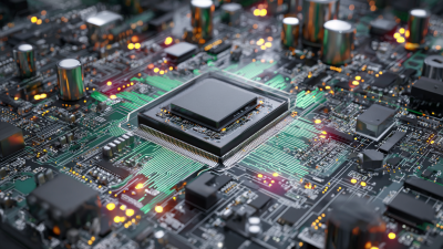
2026 Best Design PCB Trends and Techniques for Innovation?
In the ever-evolving world of technology, the "design PCB" landscape is rapidly transforming. Experts like John Smith, a leading figure in PCB design, have emphasized, "Innovation in design PCB is crucial for future advancements." As we approach 2026, it's vital to explore the trends driving this innovation.
One significant trend is the integration of smart technology within PCBs. This allows for enhanced functionality and efficiency. Designers are also focusing on sustainability. Eco-friendly materials and processes are becoming more popular. These changes, however, bring challenges that require careful consideration.
Reflecting on these trends reveals the complexities of design PCB. While advancements are exciting, they also demand a shift in thinking. How can designers balance innovation with practicality? As we navigate this dynamic field, the call for creativity and adaptability is stronger than ever. The future of PCB design is bright, yet it is not without its obstacles.

Emerging Materials in PCB Design for Enhanced Performance
Emerging materials in PCB design are shifting the landscape of electronics. Engineers are exploring innovative options to enhance performance. For example, materials like high-frequency laminates can significantly improve signal integrity. This not only benefits speed but also reduces losses.
Another fascinating option is flexible substrates. These materials allow for bendable electronics. They open new possibilities for wearables and compact devices. However, integrating this technology presents challenges. The manufacturing processes for these materials still need refinement. Adapting traditional methods to fit new designs is not straightforward.
Additionally, advanced composites are gaining traction. They combine several materials to optimize thermal dissipation. This is crucial as devices become smaller and heat management is vital. Yet, there is a learning curve in balancing durability and flexibility. Finding the right mix requires experimentation and careful consideration, leading to a potentially steep development timeline. The quest for better performance continues, revealing both opportunities and obstacles in the journey of PCB innovation.
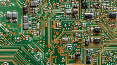
Innovative PCB Layout Techniques for Better Signal Integrity
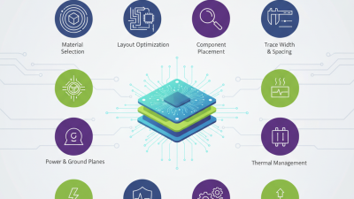
Innovative PCB layout techniques are essential for enhancing signal integrity in today's rapidly evolving electronics landscape. The growing demand for faster data transfer and improved performance is pushing engineers to explore advanced layout strategies. According to industry reports, over 70% of signal integrity issues stem from poor PCB design choices. This highlights the urgent need for innovative approaches to PCB layouts.
One effective technique is utilizing controlled impedance traces. By ensuring that trace widths and spacing are consistent throughout the board, designers can minimize reflections and maintain signal quality. Additionally, implementing proper ground planes can significantly reduce electromagnetic interference (EMI). Studies reveal that PCBs with optimized grounding can achieve up to a 30% reduction in noise levels. Yet, many designers still overlook these basic principles, leading to potential inefficiencies.
Another critical aspect is the strategic placement of components. Careful arrangement can help reduce the length of high-frequency signals, which in turn improves overall performance. However, challenges remain. It requires careful consideration of thermal management and space constraints. Designers often struggle with balancing these competing demands. Continuous learning and adaptation are crucial in this fast-paced environment. Staying current with the latest techniques can make the difference between success and costly redesigns.
Integration of Advanced Technologies for Smart PCB Solutions
The integration of advanced technologies is reshaping PCB design. Smart PCB solutions utilize digital tools to enhance functionality. For instance, embedded components can save space and reduce assembly time. This allows for compact designs that meet modern electronics’ demands. Sensors, microcontrollers, and wireless features are now commonplace.
Tips: When designing, prioritize modularity. It often reduces complexity and improves maintenance.
Artificial intelligence is also playing a critical role. AI-driven software can predict failures before they occur. This advancement helps in optimizing designs. However, reliance on AI can be a double-edged sword. Designers must ensure human insight remains. Without it, important nuances may be overlooked.
Tips: Regularly review designs with peers. Fresh perspectives often reveal hidden flaws.
Flexible PCBs are another innovation trend. They adapt better to diverse environments and applications. Though they are advantageous, the manufacturing process can be challenging. Complexities in production may lead to unexpected costs. Therefore, meticulous planning is essential in every stage.
2026 Best Design PCB Trends and Techniques for Innovation
| Trend |
Description |
Impact |
Technology |
| Flexible PCBs |
Allows for unique 3D shapes, enabling compact designs. |
Increased design freedom and reduced space. |
Polyimide materials. |
| High-Frequency PCB |
Designed for RF applications and improved signal integrity. |
Better performance in wireless communication devices. |
Low-loss dielectric materials. |
| Embedded Components |
Integrating components directly into the PCB layers. |
Reduced space and improved reliability. |
Advanced manufacturing processes. |
| AI in PCB Design |
Utilizing AI algorithms for optimized design processes. |
Faster design cycles and reduced errors. |
Machine learning technologies. |
| Sustainable Materials |
Use of eco-friendly materials and processes in PCB manufacturing. |
Reduced environmental impact and enhanced brand reputation. |
Biodegradable substrates. |
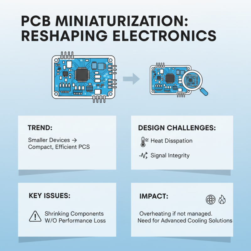
Trends in PCB Miniaturization and its Impact on Electronics Design
The trend of PCB miniaturization is reshaping electronics design. As devices become smaller, the need for compact, efficient PCBs increases. Designers face challenges when shrinking components without sacrificing performance. Heat dissipation and signal integrity are critical issues. Smaller boards can lead to overheating if not managed properly.
To navigate these hurdles, designers should consider the use of advanced materials. Flexible substrates, for example, allow for unique layouts and better thermal management. This enables innovative designs while maintaining functionality. Another technique involves incorporating multi-layer designs. It can create more space for routing without increasing the board's footprint.
Tip: Always simulate thermal performance when designing compact PCBs. It saves time and avoids costly redesigns. Additionally, focus on optimizing layout for signal integrity. Poor layout can lead to malfunction in smaller devices. Remember, innovation comes with a learning curve. Embrace trial and error in the design process. Adapt and refine your approach continuously.